RSS-Beitrag
01.04.2020 - 09:00:00
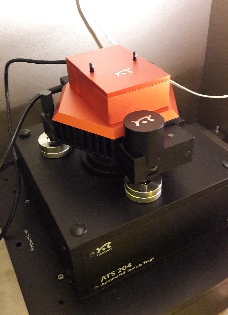
New atomic force microscope for the NanoEngineering internship
In the UDE's NanoEngineering course, students learn that the miniaturization of semiconductor components over the past decades has made it possible to create compact, high-performance components, and that new physical phenomena are sometimes encountered, but also corresponding challenges arise. Structuring and characterizing the components on this scale requires not only theory but also the appropriate manufacturing technology and equipment. Optical lithography, for example, has established itself as the method for structuring surfaces. In this process, a light-sensitive resist is exposed through a mask and the pattern of the mask is transferred into it. An alternative method is the so-called nanoimprint lithography. Here, the structure is transferred into a mechanically deformable resist by stamping and thus offers a simple method for large-area structuring.
For topological and geometrical analysis of the structures, a local resolution in the range of a few nanometers is necessary. For this purpose, a new atomic force microscope from Nanosurf was purchased. In atomic force microscopy, a 3D topographic measurement of the sample surface is performed by scanning with a nanometer-thin measuring needle. During the scanning of the surface the measuring needle is bent, which is detected by a LASER or by the deflection of the LASER. The students learn how to use the new, modern atomic force microscope and how to evaluate the measurement results.