Welcome to Electronic Materials and Nanostructures
job vacancy
[07.03.2024]
scientific staff (f/m/d No. 162-24)
at Chair of Electronic Materials and Nanostructures
follow to site for the job vacancy
or as pdf: job vacancy 162-24
job vacancy
[09.11.2023]
scientific staff (f/m/d No. 770-23)
at Chair of Electronic Materials and Nanostructures
follow to site for the job vacancy
or as pdf: job vacancy 770-23
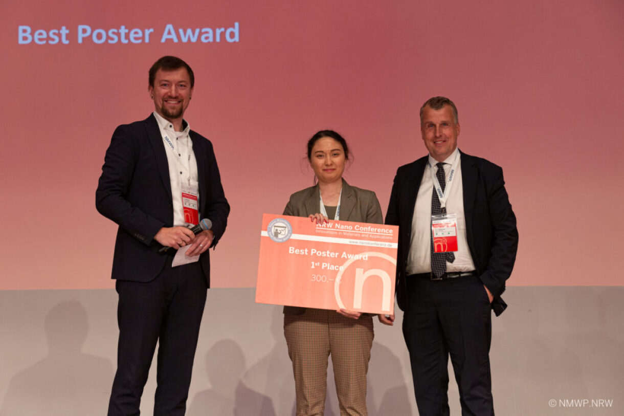
Best Poster Award for M.Sc. Tamara Czerny at 10th NRW Nano Conference
[12.06.2023]
For the poster "Efficient Narrowband Photoconductivity of the Excitonic Resonance in 2D Ruddlesden-Popper Perovskites Due to Exciton Polarons" M.Sc. Tamara Czerny was awarded the Best Poster Award at the 10th NRW Nano Conference - Innovations in Materials and Applications, May 23-24, 2023 in Dortmund. The poster is about a narrow band photodetector based on a 2D perovskite thin film and the findings on the origin of charge separation, which belongs to the topic of the working group Electroenergetic Functional Materials around Jun.-Prof. Franziska Muckel.

Dr. Pradeep Kodimana Ramakrishnan receives Walter Benjamin Grant of the German Research Foundation (Deutsche Forschungsgemeinschaft):
[02.05.2023]
The German Research Foundation (DFG) awards Dr.Pradeep Kodimana Ramakrishnan,
a postdoctoral researcher working with the group of Prof. Gerd Bacher at the Werkstoffe der Elektrotechnik, University of Duisburg-Essen, the Walter Benjamin Position for the project titled: "Demystifying the Exciton-Dopant Interaction in Lead Halide Perovskites by Magneto-Optical Spectroscopy on Single Nanocrystals"
The Walter Benjamin Programme enables postdoctoral researchers at an early career phase who are associated with a German research institution or work there, to conduct independently a research project of their choice and to benefit from additional career-promoting conditions. The award finances the position for two years while the University of Duisburg-Essen covers additional project needs. The prize is named after Walter Benjamin, a German philosopher and cultural critic, who lived from 1892-1940.
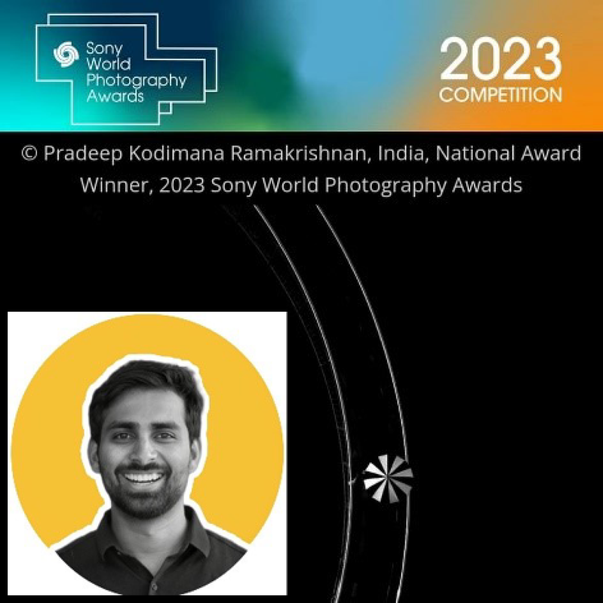
Sony World Photography Awards Dr. Pradeep Kodimana Ramakrishnan received the India National Award 2023
[14.03.2023]
Aimed at supporting the best regional photographers around the globe, the Sony World Photography Awards has released its list of this year’s National winners from a record number of more than 415,000 images from more than 200 countries and territories.
The World Photography Organisation and Sony India are delighted to announce Dr. Pradeep Kodimana Ramakrishnan, a present postdoctoral researcher at the Werkstoffe der Elektrotechnik working with the group of Prof. Gerd Bacher at UDE as India’s National Award winner for the Sony World Photography Awards 2023.
The National Awards program is an initiative set up by the World Photography Organisation and Sony to support local photographic communities around the world, with 55 countries taking part this year. Over 415,000 images from over 200 countries and territories were submitted to the Sony World Photography Awards 2023 and over 200,000 were entered to the Open competition (from which the National Awards winner was selected).
Pradeep was anonymously selected by judges for his photograph Tuffie entered the Street Photography category of the Open competition. The image depicts Navigating life’s twists and turns, one step at a time. Pradeep’s photograph is stripped to the bare minimum. It focuses solely on the minimalist lines and shapes, made even more prominent by the picture's lack of colour. It was shot at the iconic location in Duisburg, the Tiger and Turtle in the last summer. He is also a member and organizer of the Düsseldorf Street Photography group. His images were published at United Nations Climate Change Conference (COP 27) 2022. He is a self-taught photographer and has learned photography through experimenting and independent study from various online sources.
As India’s National Award winner, Pradeep Kodimana Ramakrishnan receives Sony digital imaging equipment and will be included in the Sony World Photography Awards exhibition and book. All of the award-winning images will be displayed at a photography exhibition at Somerset House in London from April 14th to May 1st.
Catalysis Success at Transregio
[27.05.2022]
Extension of a Collaborative Research Center/Transregio: The German Research Foundation (DFG) is extending the existing TRR on catalytic materials and processes for another four years.
In contrast to a classical Collaborative Research Center (SFB), a Collaborative Research Center/Transregio (TRR) is jointly applied for and supported by two or three universities. The UDE is significantly involved in the extended SFB/TRR:
Targeted design of new catalyst materials
Almost all everyday objects come into contact with at least one catalyst during their production to make production cheaper, more environmentally friendly or even possible in the first place. The development of inexpensive, highly active and selective catalysts at the atomic level is the goal of SFB/TRR 247 "Heterogeneous Oxidation Catalysis in the Liquid Phase". Following its successful first funding phase, it is being extended by the DFG for a further four years period and funded with 12.3 million euros. The researchers are now focusing on identifying active centers of the materials and understanding reaction mechanisms in detail. The Department of Electronic Materials and Nanostructures is involved in this with a project. In this project, optical spectroscopy is used to investigate catalytic processes.
In the picture: View of the center of a synthesis reactor in which nanoparticles are created and investigated within a spray flame - for example for the development of new catalyst materials. The probe projecting into the flame for sampling withstands temperatures of up to 2,600°C.
by Birte Vierjahn

Success for the UDE DFG funds an international research training group
[09.05.2022]
Materials sciences at the UDE can further expand their research. The German Research Foundation (DFG) is funding a new International Research Training Group (IRTG) with a total of around 7.3 million euros for the first five years. The research subjects are the properties and production of two-dimensional materials.
Two-dimensional (2D) materials are extremely thin and in some cases consist of only a single layer of atoms. They are particularly interesting because they have unique electrical and optical properties and can be rolled, folded or stretched due to their high mechanical stability. The IRTG Scalable 2D Material Architectures (2D-MATURE). Synthesis and Processing, Characterization and Functionality, Implementation and Demonstration at the Faculty of Engineering with participation from the Faculty of Physics will address two questions: How can two-dimensional materials be produced in large quantities, and how do they behave when combined with other materials in ways that can be used in products?
The goal is to develop new methods and processes to enable industrial-scale applications, for example in light-emitting diodes or batteries. The IRTG is headed by Prof. Gerd Bacher (Faculty of Engineering, Department of Electrical Engineering and Information Technology). The PhD students, who are conducting research at the Center for Nanointegration Duisburg-Essen (CENIDE), will collaborate with Canadian colleagues at the Waterloo Institute of Nanotechnology (WIN) at the University of Waterloo and also spend several months there.
Dr. Thomas Wittek, press office UDE
Franziska Muckel has been portrait as Research Talent at the UDE
[09.02.2022]
The WISNA-Juniorprofessor Franziska Muckel has been portraited as a Research Talent of the UDE. In this online series the UDE introduces young and up-and-coming researchers of various disciplines. In a three-part video series, Franziska Muckel discusses what’s crucial for material development, why she has returned to the UDE and that she initially planned to work on a ship rather than in the lab.
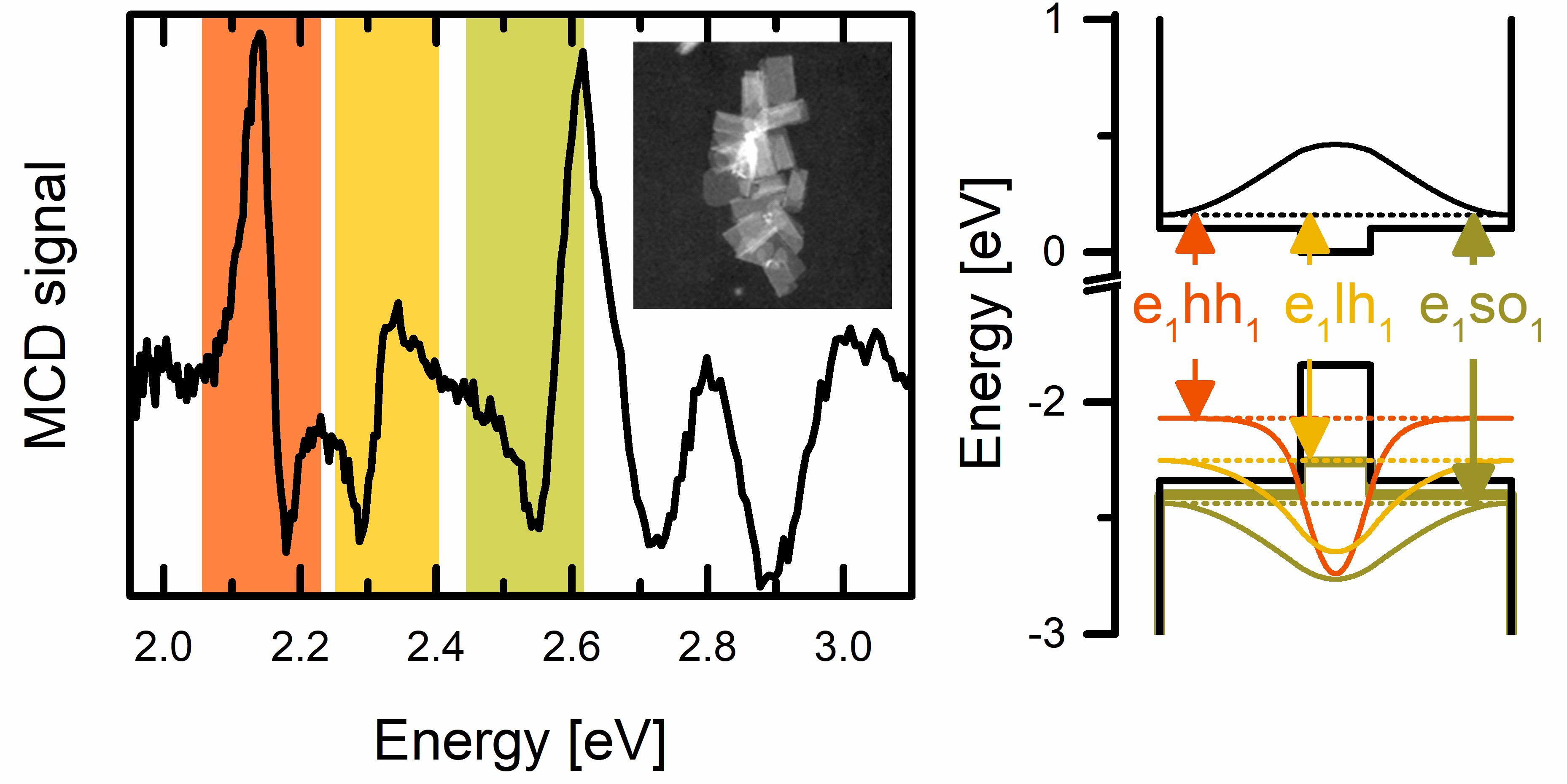
Crystallographic Insights by Optical Spectroscopy on the Nanoscale
[07.02.2022]
Being 10.000 times smaller than a human hair, they have the potential to revolutionize the world of light emitting devices: Semiconductor crystals from a novel semiconductor material – so-called perovskites – with sizes of only few nanometers promise record efficiencies, outstanding stability, and unprecedented scalability. Scientist of the Center for Nanointegration (CENIDE) at the University of Duisburg-Essen (UDE) and collaborators have now found a way to determine the crystallographic properties of such nanocrystals using solely spectroscopic methods – featured in the journal “Nano Letters”.
Despite setting countless records in the fields of photovoltaics and light emission for several years, the microscopic origin of the outstanding properties of the perovskite semiconductor material class is still subject of lively scientific debates to date. Scientists at the chair for „Electronic Materials and Nanostructures“ collaborate with a partner group at the ETH Zurich to investigate the optical properties of tiny perovskite crystals, so-called quantum dots, and their correlation with the atomic structure of the semiconductor material.
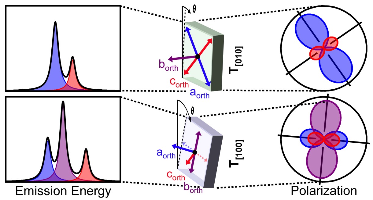
In a recent publication, the group demonstrated the determination of the atomic crystal structure of asymmetric nanocrystals with dimensions of only 10x3 nanometers by purely analyzing the light emission of the crystals. This direct connection, which does not hold in classical semiconductors and symmetric nanostructures, enabled detailed insights into the correlation between the atomic structure and the optical properties of the promising semiconductor. Additionally, the scientists succeeded to reconstruct the spatial orientation of individual nanocrystals from purely optical measurements, enabling the assignment of the optical signals to the respective crystal axes for the first time.
The observation of these correlations highlights the potential of such asymmetric perovskite nanocrystals to guide the scientific community towards unraveling the intriguing properties of this material system and to transfer this knowledge to potential new, and even better, semiconductor systems.
Original publication:
A. Schmitz et al., Nano Lett. 21, 9085 (2021)
[DOI: 10.1021/acs.nanolett.1c02775]
Research projects in cooperation with the University of Waterloo in Canada
[04.02.2022]
In late fall of last year, two of our scientists moved their workplace to Canada for a few weeks to carry out experiments for their PhD research.
Within the DAAD program for project-related personal exchange, the cooperation with the University of Waterloo strengthened the international network of our group. In the lively scientific exchange between the researchers on site, they worked on the continuous development of optoelectronic devices based on 2D materials. M. Sc. Henrik Myja combined different fabrications methods in order to embed 2D semiconductors in LED architectures. On the one hand, current injection layers of conducting oxides were deposited by a system for large area atomic layer deposition at atmospheric pressure (AP-SALD) in the group of Prof. Kevin Musselman. This was complemented by contact layers of silver nanowires from Prof. Irene Goldthorpe's group. With this combination, he succeeded in producing transparent LEDs.
M. Sc. Yannick Beckmann worked on the encapsulation of detectors based on 2D materials. For this, also in collaboration with Prof. Musselman's group, he deposited different oxides on his devices using AP-SALD and was thus able to significantly improve the sensitivity of his photodetectors.

Franziska Muckel becomes member of the Young College
[28.01.2022]
Starting January 2022, Jun.-Prof. Franziska Muckel joins the Young College (“Junges Kolleg”) of the Nort-Rhyne-Westphalian Academy for Science and Arts.
The Young College was founded in 2006 and serves as a platform for free research and interdisciplinary dialogue. The membership, which is granted for up to four years, represents a high distinction and comes with a annual scholarship of € 10.000 to support the young researchers and artists. Besides getting in contact with young researchers from various disciplines, the members get the chance to participate in all events of the Academy for Science and Arts, especially the scientific sessions of the different disciplines.
News UDE : new member of the Young College
Two-Dimensional (2D) Magnets
[26.01.2022]
Starting with the pereparation of graphene (an atomically thin carbon layer) in 2004, two-dimensional materials have been playing an important role in the research for electronic and optical applications. Meanwhile, more than 1000 different 2D materials have been predicted (and partly realized). In addition to graphene, isolating or semiconducting 2D materials are highly attractive for future electronic components like transistors, LEDs or solar cells.
It took until 2017 for first inspiring reports on distinct magnetic properties in pristine single layers of 2D materials. This discovery opens a complete novel field of research on 2D materials, especially since different 2D materials can be stacked in top of each other to create heterostructures with completely new physical properties.
In collaboration with Prof. Doron Naveh (Ramat-Gan, Israel), Prof. Efrat Lifshitz (Haifa, Israel) und Prof. Thomas Heine (Dresden, Germany) our group will continue the research on this trendsetting subject within a new project of the German-Israeli Project Coordination (DIP), a program by the German Research Foundation (DFG). The work will investigate heterostructures of 2D antiferromagnetic (AFM) semiconductors with valley-polarized transition metal dichalcogenides or / and 2D superconductors. We aim to control the heterostructures’ magnetic properties by tuning the strength and nature of interlayer interactions.

Research on Semiconductors Light Weakens Magic Nanoclusters
[21.01.2021]
They are known as "magic sized nano clusters" because they have special properties: The particles consist of only a few atoms, but since they are arranged in a special crystal structure, they are extremely stable. Unless you expose them to light.
Scientists from the Center for Nanointegration (CENIDE) at the University of Duisburg-Essen (UDE) have discovered that such materials undergo fundamental changes as soon as they are merely analysed using optical methods. "Nature Communications" reports on the issue.
Junior professor Dr. Franziska Muckel is head of the working group "Electroenergetic Functional Materials" at the chair "Materials of Electrical Engineering”. Her team investigates cadmium selenide particles, which consist of no more than 26 atoms. Yet these atoms are arranged in a crystal structure, i.e. in a regular lattice similar to the symmetrical climbing frames made of ropes and metal on children's playgrounds. This structure renders the particles extremely stable.
In collaboration with the Seoul National University (South Korea) and the Max-Planck-Institut für Eisenforschung in Düsseldorf, UDE's researchers demonstrated that light above a certain wavelength weakens the bonds within these semiconductor nano clusters significantly – a hundred times more than in the same material with much larger dimensions.
Optical analysis methods as standard techniques in semiconductor research thus reach their limits in these dimensions: Instead of merely elucidating material properties, they change the investigated material itself. Since magic nano clusters are an important intermediate step on the way to larger functional particles, this is a decisive discovery.
Muckel, who conducts her research at the NanoEnergieTechnikZentrum (NETZ) on the Duisburg campus, now wants to put the results to practical use: "In the long term, we plan to develop components from similar materials that convert light into charge carriers and could therefore serve as optical sensors."
Original publication:
F. Muckel et al., Nat Commun 11, 4127 (2020)
[DOI: 10.1038/s41467-020-17563-0]
Master thesis sponsored by the Stiftung Industrieforschung
[24.09.2020]
Every year, the Stiftung Industrieforschung supports students from technical and scientific studying programs throughout Germany whose master's thesis promises relevance to medium-sized industrial companies with a scholarship.
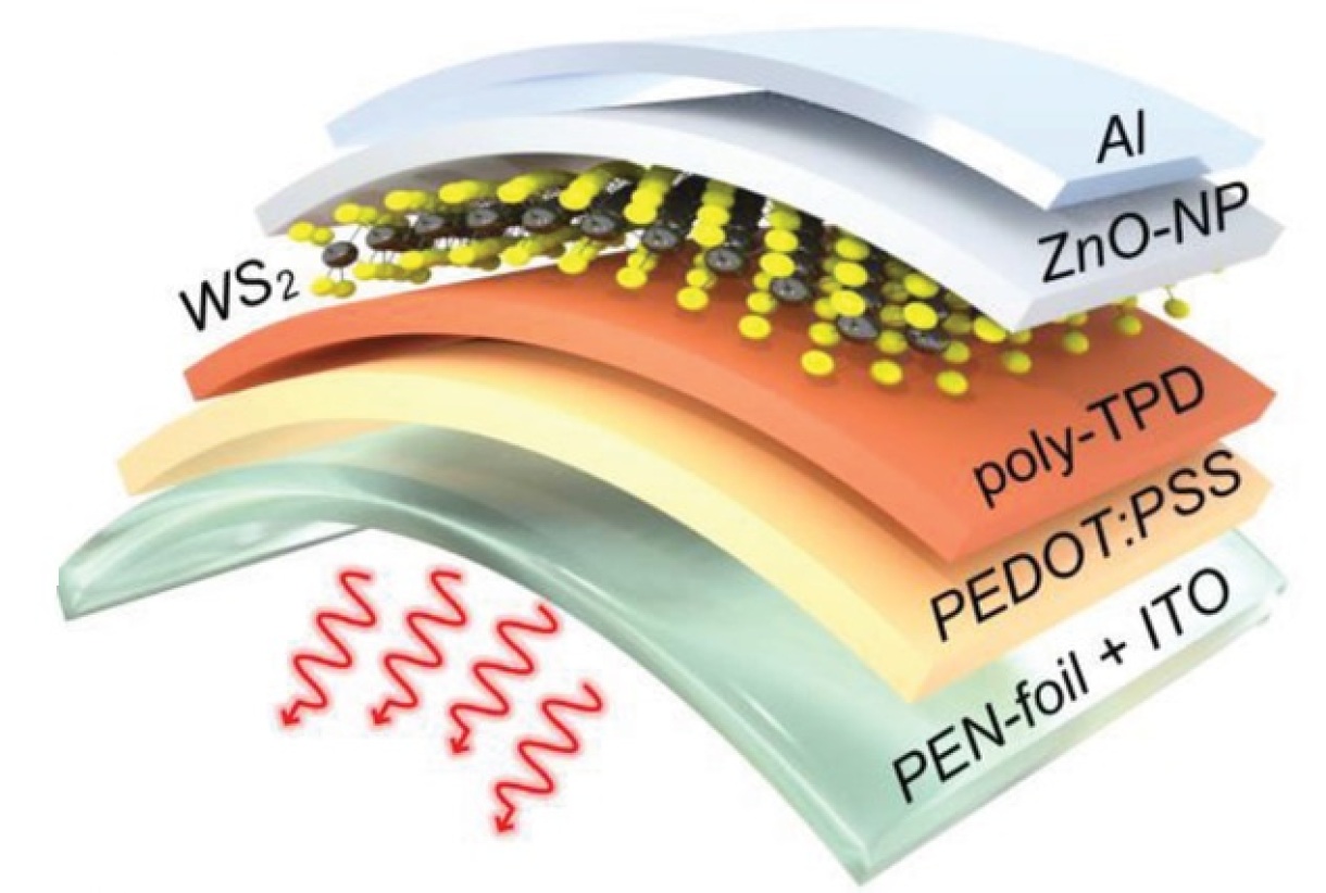
B.Sc. Henrik Myja receives one of these coveted scholarships for his thesis on "Transparent and flexible light emitting devices based on nanometer-thin 2D semiconductors" at the Chair of Electronic Materials and Nanostructures (Prof. Dr. Gerd Bacher). The active material used for the devices are large-area tungsten disulfide monolayers, which originate from a cooperation with Prof. Dr. Andrei Vescan from the RWTH Aachen University. These are investigated with respect to internal quantum efficiency and embedded in to a transparent and flexible device environment. The analysis of the devices will be used to estimate the application potential, e.g. in the field of flexible lighting or display elements for weight-reduced mobile solutions.
Creating magnetism from light!
[02.04.2020]
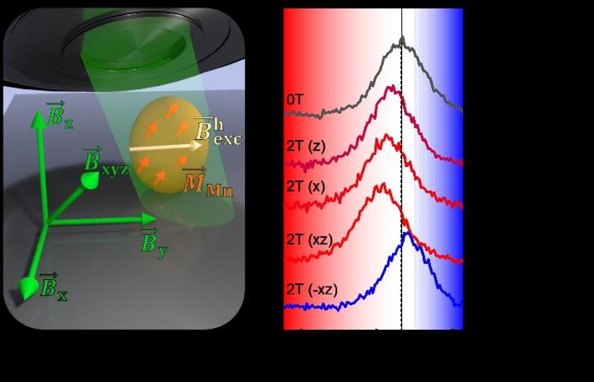
Generating magnetism on demand without the use of electrical currents – in the field of doped nanocrystals no science fiction anymore, but close to reality. A major breakthrough in this area was recently achieved by the group of Prof. Gerd Bacher in collaboration with the Gamelin Group at the University of Washington, Seattle.
Using spectroscopy on individual nanocrystals in a rotatable magnetic field it was shown how light induced magnetism can be purposefully directed.
In future, this work will be continued and extended with funding of the Deutsche Forschungsgemeinschaft, which has just granted a full 3 year project on this topic.
Original publication:
S. Lorenz et al., Nano Letters 20, 1896 (2020)
[DOI: 10.1021/acs.nanolett.9b05136])
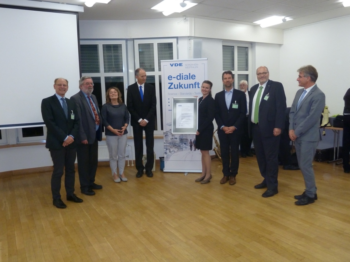
VDE Promotion Award 2019 for Dr. Franziska Muckel
[20.11.2019]
This year's VDE Promotion Award, endowed with 3,000 Euro, was presented to Dr. Franziska Muckel for her dissertation "Magnetically doped semiconductor quantum dots from solvent-based production: from functionality to device" in a ceremony at the Gerhard Mercator House in Duisburg.
During her doctorate, Ms. Muckel developed semiconductor nanocrystals that combine electrical, optical and magnetic functions in a very small space. With this basic research, many devices will soon be even more powerful. Since its foundation, VDE Nordrhein-Westfalen has donated an annual doctoral prize for special achievements in the fields of electrical engineering, electronics and information technology to female scientists at the universities of Aachen, Bochum, Duisburg, Dortmund, Hagen, Paderborn, Siegen and Wuppertal. In addition to the scientific originality and innovative value of the submitted work, the applicability and relevance of the results for the state of North Rhine-Westphalia are also examined and evaluated.
by Siegbert Kmetz
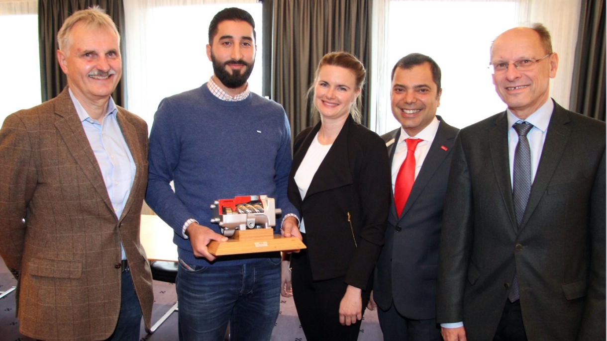
Innovation Prize of the Sparkasse am Niederrhein for Dr. Franziska Muckel
[13.11.2019]
For her dissertation entitled "Transition Metal Doped Colloidal Semiconductor Nanocrystals: From Functionality to Device Development" Dr. Franziska Muckel was awarded the coveted innovation prize of the Sparkasse am Niederrhein.
Ms. Muckel developed semiconductor nanocrystals that combine electrical, optical and magnetic functions in the smallest of spaces. With this basic research, many devices will soon be even more powerful". For more than 20 years, the Sparkasse, in cooperation with the in Moers-based development association for engineering sciences, has been honoring application-related and outstanding dissertations and master's theses written in the engineering sciences of the UDE.
Best PhD Student Oral Contribution Award for transparent graphene electrodes on GaN based LEDs
[29.6.2019]
For the conference contribution „Direct growth of graphene on GaN under N2 atmosphere“ M.Sc Jan Mische was priced with the Best PhD Student Oral Contribution award at Graphene2019.
In his talk he spoke about the direct growth of graphene via plasma enhanced chemical vapor deposition (PECVD) on GaN based LEDs. Goal of the work is to get graphene utilize as a transparent electrode for LEDs, which would increase the efficiency.
Graphene2019 [Awards]

ACS Photonics Poster Award for Hybrid QD-LECs
[29.7.2018]
M. Sc. Julia Frohleiks was honored with the ACS Photonics Poster Prize and a reward of 1000 US-Dollar for her poster entitled „Hybrid Quantum Dot – Light-Emitting Electrochemical Cells“ in context of QD2018 – the 10th Biannual Conference on Quantum Dots in Toronto (Canada).
Julia Frohleiks, a member of the junior research group Solid State Lighting (Dr. E. Nannen) and the department for electronic materials and nanostructures (Prof. G. Bacher), develops innovative light-emitting devices. These hybrid devices are a combination of light-emitting semiconducting nanocrystals (quantum dots, QDs) and light-emitting electrochemical cells (LEC). The poster shows the results on devices that use colloidal QDs to supplement the LEC emission color as well as on devices that replace the LEC emitter completely and show light emission solely of the light-emitting QDs.
Further details on the results can be found in ACS Applied Materials & Interfaces 8, 24692 (2016), LED Lighting Technologies – Smart Technologies for Lighting Innovations, Luger Research e.U., 206 (2017) and Advanced Materials Technologies 2, 1700154 (2017).
New special research field at UDE with involvement of Electronic Materials and Nanostructures
[17.05.2018] The German Research Foundation DFG is funding a new Collaborative Research Center "Heterogeneous Oxidation Catalysis in the Liquid Phase" under the umbrella of the University Alliance Ruhr with approximately € 10 million for the first four years. Spokesman is Prof. Malte Behrens from the Faculty of Chemistry. The WET is also on board. In the coming years we will investigate charge carrier dynamics in oxide photocells with spinel and perovskite crystal structures.
Successful Cooperation with Technical University Nanyang, Singapore
[09.05.2018]
A scientific breakthrough in the area of doped nanocrystals has been achieved in a collaboration between the Chair of Electronic Materials and Nanostructures in Duisburg and colleagues from the Technical University Nanyang in Singapore.
Semiconductor nanoplatelets with a thickness of only a few monolayers could be doped with transition metal ions quite precisely resulting in an extraordinary magneto-optical functionality. The unique architecture of the nanoplatelets allowed to adjust the coupling between magnetic and optical properties and to elucidate the electronic structure of these advanced nanomaterials with exceptional accuracy. These results have been published in the high impact journal Nano Letters.
This publication represents the starting point for an ongoing collaboration between the partners in this fascinating area of research, which will be supported by the Deutsche Forschungsgemeinschaft in the frame of a novel research project granted for 3 years just recently.
Original publication:
F. Muckel et al., Nano Letters 18, 2047-2053 (2018)
[DOI: 10.1021/acs.nanolett.8b00060]
University of Duisburg-Essen (UDE)
Campus Duisburg
Faculty of Engineering
Departement of Electrical Engineering and Information Technology
Electronic Materials and Nanostructures
Prof. Dr. rer. nat. Gerd Bacher
(chair holder)
Bismarckstraße 81 ( BA )
47057 Duisburg
Jun.-Prof. Dr. rer. nat. Franziska Muckel
Carl-Benz-Straße 199
47057 Duisburg
Secretary
Phone: 0203 / 379 - 3405
Fax: 0203 / 379 - 3404
E-mail: petra.merker@uni-due.de
Selection of recent publications
Alexander Schmitz, Federico Montanarella, L. Leander Schaberg, Mohamed Abdelbaky, Maksym V. Kovalenko, and Gerd Bacher
"Optical Probing of Crystal Lattice Configurations in Single CsPbBr3 Nanoplatelets"
Nano Lett. (2021), [DOI: 10.1021/acs.nanolett.1c02775]
Franziska Muckel, Kathryn N. Guye, Shaun M. Gallagher, Yun Liu, and David S. Ginger
"Tuning Hybrid exciton–Photon Fano Resonances in Two-Dimensional Organic–Inorganic Perovskite Thin Films"
Nano Lett., 21, 14, 6124–6131 (2021), [DOI: 10.1021/acs.nanolett.1c01504]
U. Hutten, L. Daniel, A. Grundmann, N. Stracke, M. Abdelbaky, Y. Beckmann, M. Heuken, W. Mertin, H. Kalisch, A. Vescan, G. Bacher, T. Kümmell
"Transfer-free, scalable photodetectors based on MOCVD-grown 2D-heterostructures"
2D Materials 8, 045015 (2021), [DOI: 10.1088/2053-1583/ac186d]
Severin Lorenz, Jan Bieniek, Christian S. Erickson, Daniel R. Gamelin, Rachel Fainblat and Gerd Bacher
"Orientation of Individual Anisotropic Nanocrystals Identified by Polarization Fingerprint"
ACS Nano, 15, 13579-13590 (2021), [DOI: 10.1021/acsnano.1c04451]
L. Kampermann, J. Klein, J. Korte, O. Kowollik, O. Pfingsten, T. Smola, S. Saddeler, T.H. Piotrowiak, S. Salamon, J. Landers, H. Wende, A. Ludwig, S. Schulz, G. Bacher
"Link between structural and optical properties of CoxFe3-xO4 nanoparticles and thin films with different Co/Fe ratios"
J. Phys. Chem. C 125, 14356 (2021), [DOI: 10.1021/acs.jpcc.0c11277]
F. Muckel, S. Lorenz, J. Yang, T. A. Nugraha, E. Scalise, T. Hyeon, S. Wippermann, G. Bacher
"Exciton-driven change of phonon modes causes strong temperature dependent bandgap shift in nanoclusters"
Nature Comm. 11, 4127 (2020), [DOI: 10.1038/s41467-020-17563-0]
D. Andrzejewski, R. Oliver, Y. Beckmann, A. Grundmann, M. Heuken, H. Kalisch, A. Vescan, T. Kümmell, G. Bacher
"Flexible large-area light-emitting devices based on WS2 monolayers"
Adv. Optical Mater. 2000694 (2020), [DOI: 10.1002/adom.202000694]
All publications of our department [HERE]