Homogeneous Organic Layers
Homogeneous but also polymorph

The recipe sounds simple: You have to take a clean single crystal surface and add some organic molecules by vapour depositon. The result of this procedure is very complex: you will find not only one structure but a whole bunch of them. That's what crystallographs call polymorphism. As the organic molecules are much bigger than the pattern given by the metallic substrate there are a lot of configurations with similar energies of adsorption.
Starting with the first layer ...
3,4,9,10 perylene-tetracarboxylic-dianhydride (PTCDA) on Cu(111)1 is a good example for polymorphism in a twodimensional structure: Within the first layer of PTCDA you can find two different arrangements of the molecules. Both are given by unit cells which contain two molecules rotated by about 90°. These structures are understood by taking the partial charges of the molecule into account. These herringbone-like structures are also known for the PTCDA bulk. However, there is a small difference in their geometry (size, orientation of the molecules) between the bulk and the first layer. You can explain the difference by the additional substrate-adsorbate interaction of the first layer.

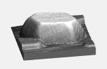
Nanocrystals are different from macroscopic ones
Between the atoms of the substrate and the molecules within the third or even higher layers there is no direct interaction any more. Due to this leak of interaction the structures for thick films (more than 10 layers) should not be affected by the substrate any more. It is expected that the structure of thick films becomes somewhat bulk-like as this represents an energetic minimum.
By means of STM, we have imaged several PTCDA crystals on Cu(110), Cu(111), Ag(111), and Au(111)2. We have found a crystal with lateral dimensions up to 500 nm and a height which is equivalent to about 100 molecular layers. The specially optimized low current STM, which can be operated with tunneling currents down to 1 pA, allowed us to image to the topmost layer and the facets of the crystals with molecular resolution. The high quality of the images allowed the three-dimensional reconstruction of the crystal. One result of this analysis is that not all nanocrystals show a structure which is similar to the bulk ones.
Publications within the project
1"The initial growth of PTCDA on Cu(111) studied by STM",
Th. Wagner, A. Bannani, C. Bobisch, H. Karacuban, R. Möller,
J. Phys.: Condens. Matter 19 (2007) 056009
2"Growth of 3,4,9,10-perylene-tetra-carboxylic-dianhydride crystallites on noble metal surfaces",
Th. Wagner, A. Bannani, C. Bobisch, H. Karacuban, M. Stöhr, M. Gabriel, and R. Möller,
Organic Electronics 5, 35-43 (2004)