ICAN: Transmission electron microscopy
What is a transmission electron microscope?
Transmission electron microscopy (TEM) is a versatile characterization method featuring highest spatial and energetic resolution. Samples need to be electron transparent i.e. their thickness must be below 100 nm. The Jeol JEM-2200FS is capable of conventional TEM as well as scanning TEM (STEM). In the STEM mode the spherical aberration of the electromagnetic lens system is corrected utilizing a CEOS double hexapole corrector enabling a resolution limit of one Angström. At the same time and resolution analytical methods like electron energy loss spectroscopy and energy dispersive x-ray spectroscopy are available.
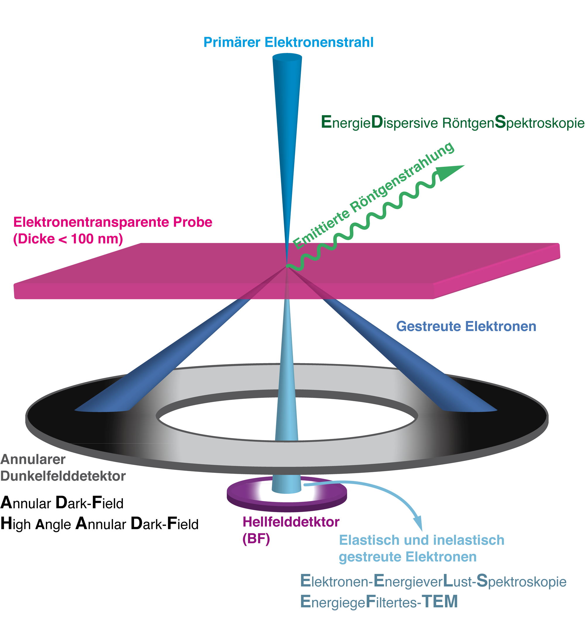
In figure 1 the interaction of sample and electron beam is sketched.
Electron diffraction
Electron diffraction reveals the crystal structure and symmetry of the sample material. In the selective area diffraction (SAD) mode the lateral resolution is limited by the size of the selection-aperture going down to ~ 250 nm. For higher lateral resolution convergent beam electron diffraction (CBED) is also possible reaching a resolution of a few nanometers.
High resolution imaging
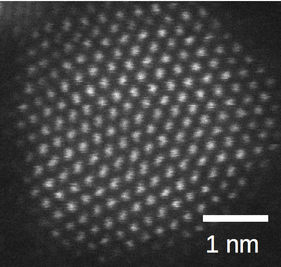
HRTEM
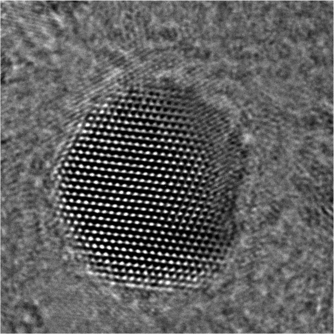
In TEM mode the sample is illuminated with a parallel beam of electrons. Depending on the sample quality imaging of atomic structures is possible ( see figures 2 and 3). At the ICAN the best achievable point resolution in TEM mode is 0.14 nm. Quantitative analysis of the exit wave is also possible using focal series reconstruction.
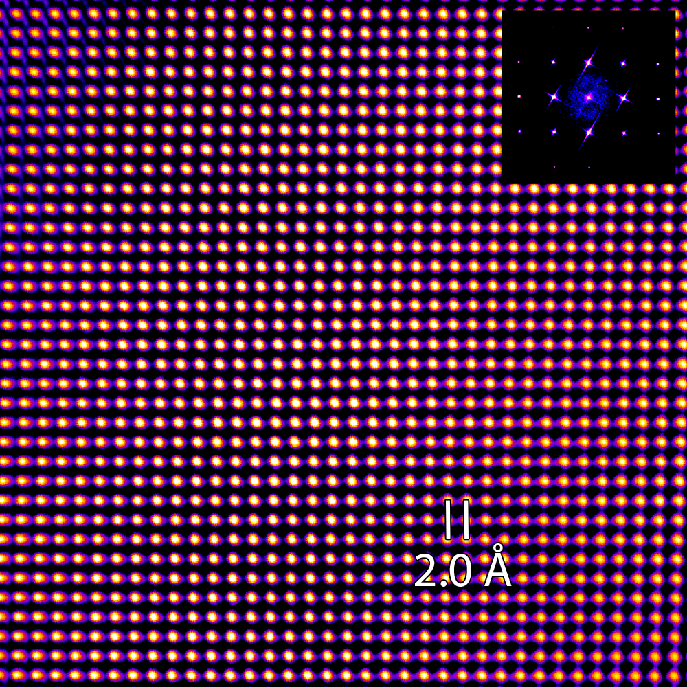
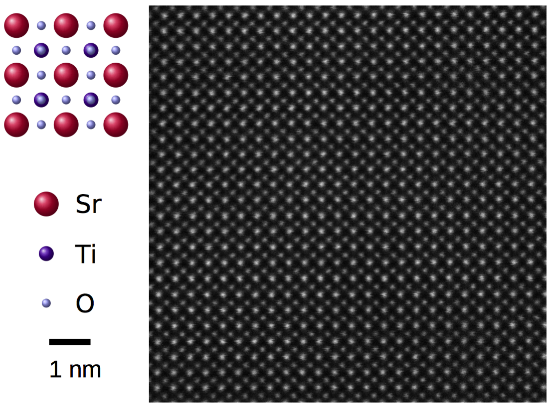
HRSTEM
In STEM mode (scanning) the electron beam will be focussed to a spot with approximately one Angström in diameter (the electron probe). This probe is than scanned across the sample in a raster fashion while the transmitted electrons can be captured using a wide variety of different detectors. With the help of the electron optical corrector the resolution in STEM mode reaches 0.1 nm. One benefit of high-angle annular dark-field (HAADF) images in the STEM mode is the proportionality of the image intensity to the atomic number Z. Therefore a direct interpretation of the elemental distribution is possible like for example contrast changes for Strontium and Titanium in figure 4 showing SrTiO3.
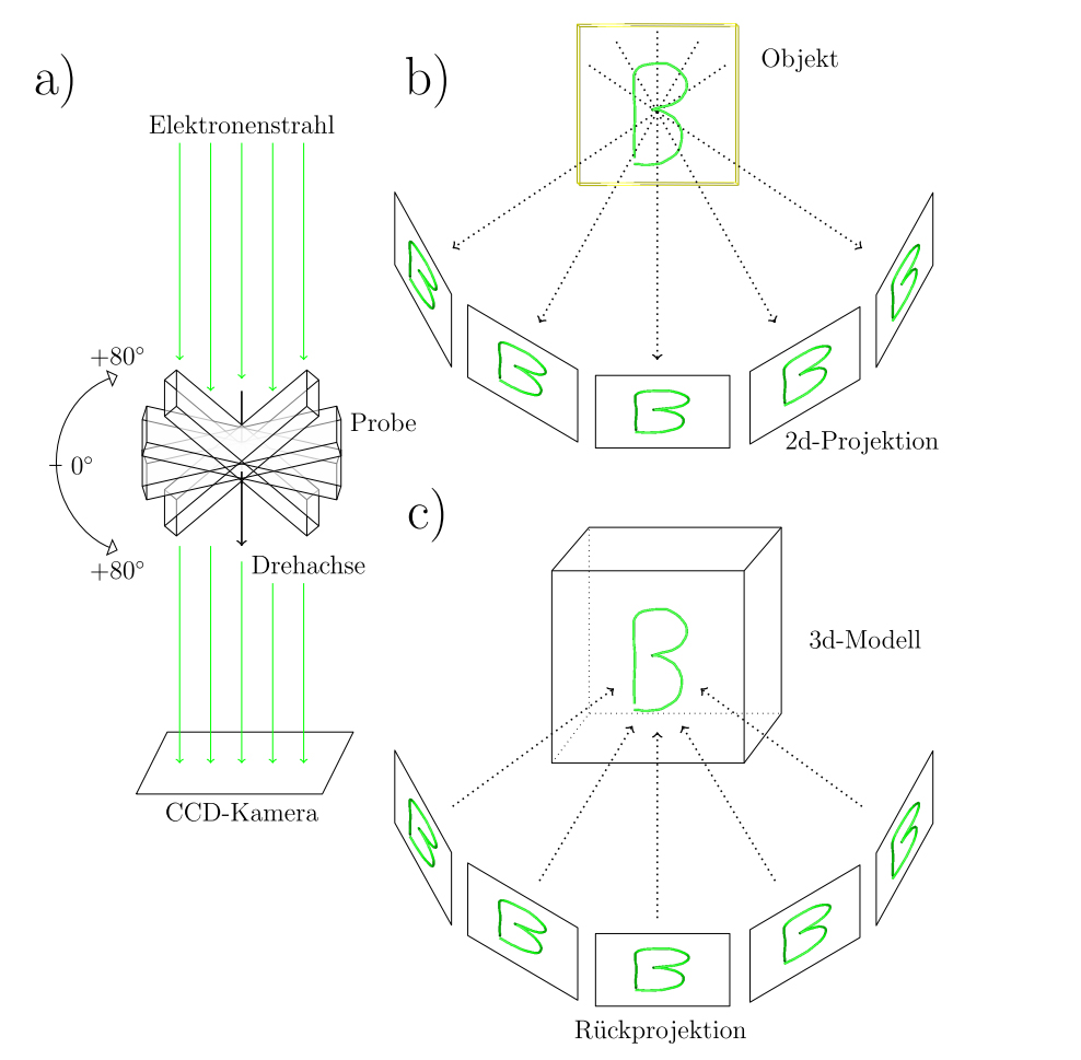
Tomography
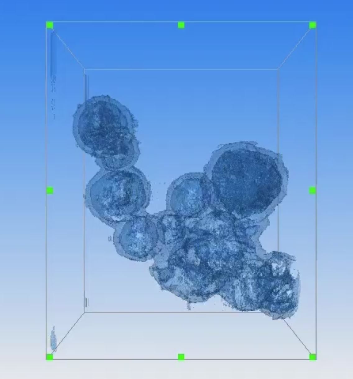
For a characterization of the 3-d structure it is necessary to acquire a tomographic tilt series at first, i.e. image the sample at different angles of projection. Typically a such a tilt series is acquired with steps of one degree from +80° to -80° angle between sample and incoming electron beam (see figure 6). At the ICAN a special tomography needle holder is also available allowing for a 360° rotation reducing artefacts (missing wedge) in the reconstruction. An exemplary tilt series of core-shell nano-particles is seen in figure 7. Different methods like weighted back projection or simultaneous iterative reconstruction are then used to create a three-dimensional model of the sample structure figure 8).

Analytic TEM
Energy Dispersive X-ray spectroscopy
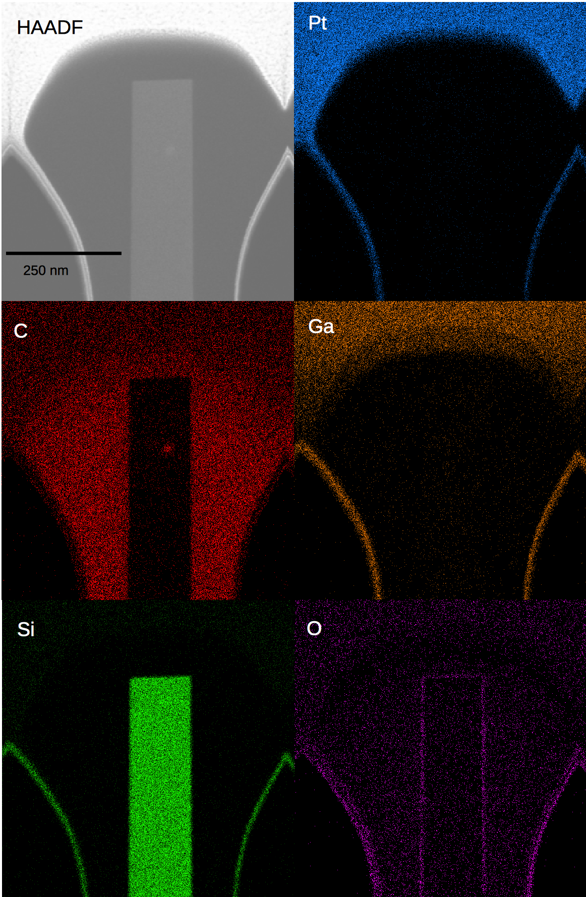
Resulting from inelastic interaction electrons of the sample material may be excited to higher energy shells or even removed from their original atomic core. By this means holes are created in the shell-structure which than get re-populated by electrons from higher shells losing their excess energy in the form of x-rays. The emitted x-rays are element-specific enabling a quantitative chemical analysis with high spatial resolution. An exemplary elemental map is shown in figure 9.
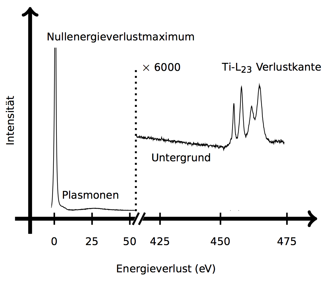
Electron Energy Loss Spectroscopy
After interaction with the shell electrons, the primary electrons lost a specific amount of energy themselves. This loss of energy is again element specific and depends on the energy difference of the excitation. Using an electromagnetic prism the energy loss of the primary electrons may be analyzed revealing not only elemental composition but also chemical bonding in the nanometer regime. In figure 10 the Ti-L23 edge is shown. The number and separation of the four peaks allows the identification of the number of oxygen atoms the titanium is bond to.
![]()

