Electrical Conductivity on the Atomic Scale
Electrical Conductivity on the Atomic Scale
Method
The aim of this experiment is a deeper understanding of the electrical conduction down to the atomic scale.
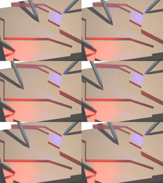
In principle two tips (1) and (3) are brought into contact with a surface in a well defined manner. A voltage between these two small contacts leads to a distribution of the potential along the surface. With an additional tip (2) the potential can be mapped.

The combination of high resolution STM and the potentiometry technique provides us with a powerful tool to explore the nature of the electrical conduction down to the atomic scale.
The only thing that has to be taken care of is that the processes of interest are located at surface and not in the bulk. In the case of a very thin conducting film on top of a negligibly conducting substrate the path of the current and therefore the local distribution of the potential depends very strongly on the morphology of the surface. On the atomic scale changes of the morphology for example are adsorbents, defects, grain boundaries, and step edges.
