Research
Cooperations

Universität Duisburg-Essen Center for Nanointegration
Research Topics
Electronic Properties of Heterostructures

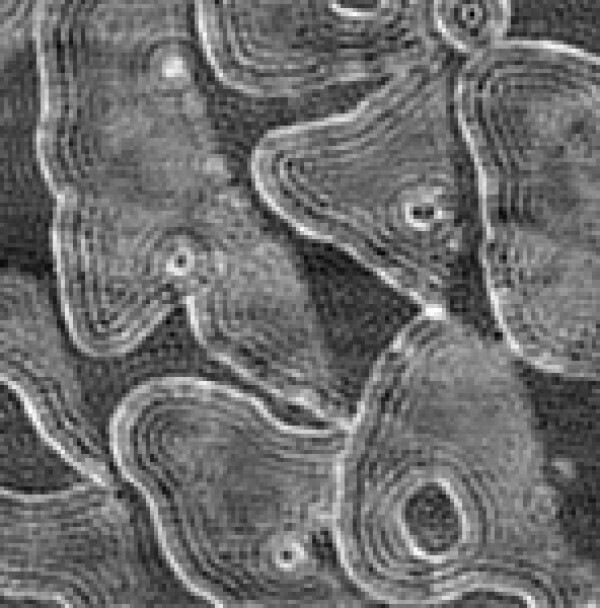
Electrons at surfaces or in thin films can be restricted in their movement. This confinement leads to special quantum mechanical states. We investigate the electronic properties changed by these low-dimensional electrons by measuring the thermovoltage across the tunneling gap of a scanning tunneling microscope.
Contact electrification

Contact electrification and triboelectricity are ubiquitous phenomena which are well known in daily life, e.g. encountering an electric shock when touching a door handle. However, the detailed processes are still not yet fully understood.
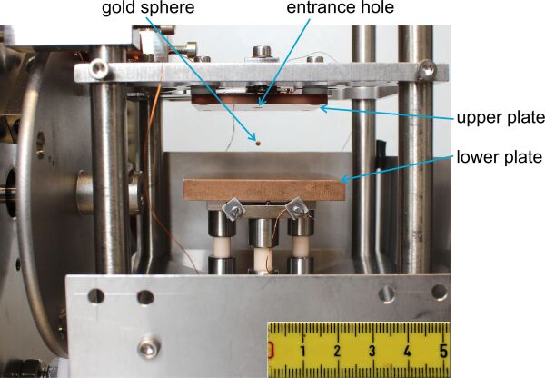
In our group, we have developed a new experimental technique which enables us to study in great detail the charge transfer occurring when two objects come into contact. It relies on new electronic charge amplifiers that measure very small charges on a time scale of microseconds. To study the contact electrification a ball with a diameter of 1 millimeter is dropped onto a plate from a height of a few centimeters, so that it bounces several times. By measuring the charge induced in the plate, it can be analyzed how the charge changes each time that it comes into contact with the surface.
The photo shows the inner part of the experimental setup. The wheel at the left side is used to transport the sphere to the upper level. A ball track, which is not visible, here guides the spheres to the entrance hole of the upper plate of the parallel plate capacitor. The lower plate is connected to a charge sensitive amplifier measuring the induced charge.
Terahertz STM

Ultrafast dynamics of adsorbed nanoobjects
Scanning tunneling microscopy (STM), owing to its high spatial resolution (sub nanometer), is a tool of choice to investigate, address and manipulate single nanoobjects adsorbed on surfaces. Many of the investigated nanoobjects, be it atoms, molecules or nanostructures, exhibit rich dynamics such as charge transfer, spin/vibration excitation and change of conformation, which are usually too fast to be resolved using typical STM instrumentation. This is because the main quantity being measured, the tunneling current, is relatively small (sub nanoampere), and its detection is typically slow (time resolution on the order of millisecond for conventional instruments).
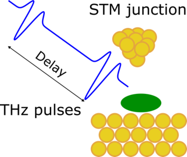
To overcome the time resolution of the detector, measurements can be performed in a stroboscopic manner as done in the field of ultrafast optics. Pump and probe voltage pulses, with an adjustable delay between them, are repeatedly applied to the sample. The dynamics of the investigated systems are inferred from the evolution of the corresponding quasi-static tunneling current as a function of the delay between the pulses. Loth and coworkers have implemented this concept in STM using an all-electronic scheme [LOT10]. They reached a time resolution on the order of 10 ns, which is essentially dictated by the ability of the wires to transmit fast pulses with limited distortion. To overcome limitations due to the wiring, Cocker and coworkers used electromagnetic THz pulses to effectively induce ultrafast voltage transients in the STM junction [COC13], which was for instance employed to track the ultrafast motion of a single molecule with a sub-picosecond time resolution [COC16].
In a close collaboration with the group of Manuel Gruber, we are implementing THz STM on a custom-made STM and using commercial THz emitters. We aim at investigating various ultrafast dynamics of individual adsorbates on surfaces at variable temperatures (10 to 300 K) under ultra-high vacuum.
[LOT10] Loth et al., Science 329, 1628 (2010).

