ICAN: Scanning augerelectron microscopy
What is scanning auger microscopy?
A scanning auger microscope (SAM) combines the scanning power and spatial resolution of a scanning electron microscope (SEM) with the element specific analysis of auger electron spectroscopy (AES). In this way it is possible to record chemical 2D maps of the chemical configuration of a surface with a spatial resolution of ~7nm.
An electron beam is rastered across the sample surface. In reacting with teh surface atoms slow moving secondary electrons as well as auger electrons are created. The detecion of the secondary electrons gives an image of the surface. Auger electrons have a kinetic energy that is element specific and hence a spectroscopic analysis of the emitted electrons allows the determination of the chemical composition of the surface.
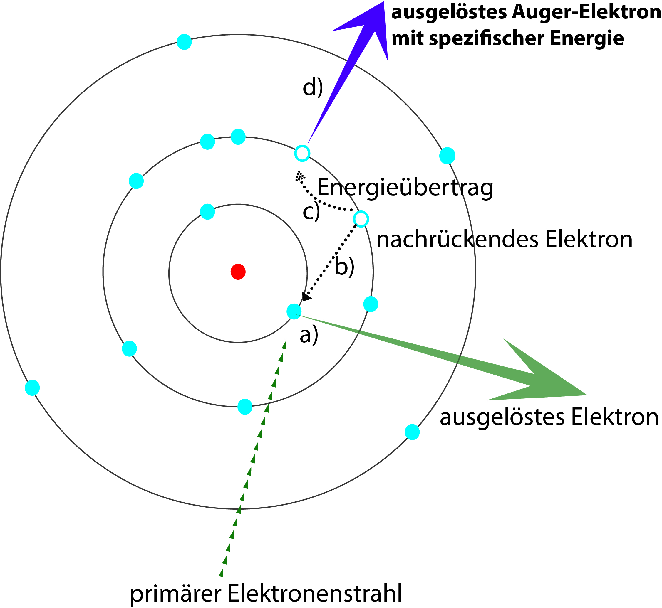
The auger proces is scetched in FIgure 1. a) An electron of the primary beam hits an electron of a surface atom which is then emitted into vacuum. b) The hole is filled by an electron from a less strongly bound shell. c) The energy, that is released by this second electron is transmitted to a third electron from the same orbital. The kinetic energy of this electron is hence only dependent on the energy difference of the different orbitals and thus element specific. d) This electron is being emitted into vacuum and detected.
At ICAN we use the Scanning Auger NanoProbe 710 by Ulvac-Phi.
Chemical 2D maps
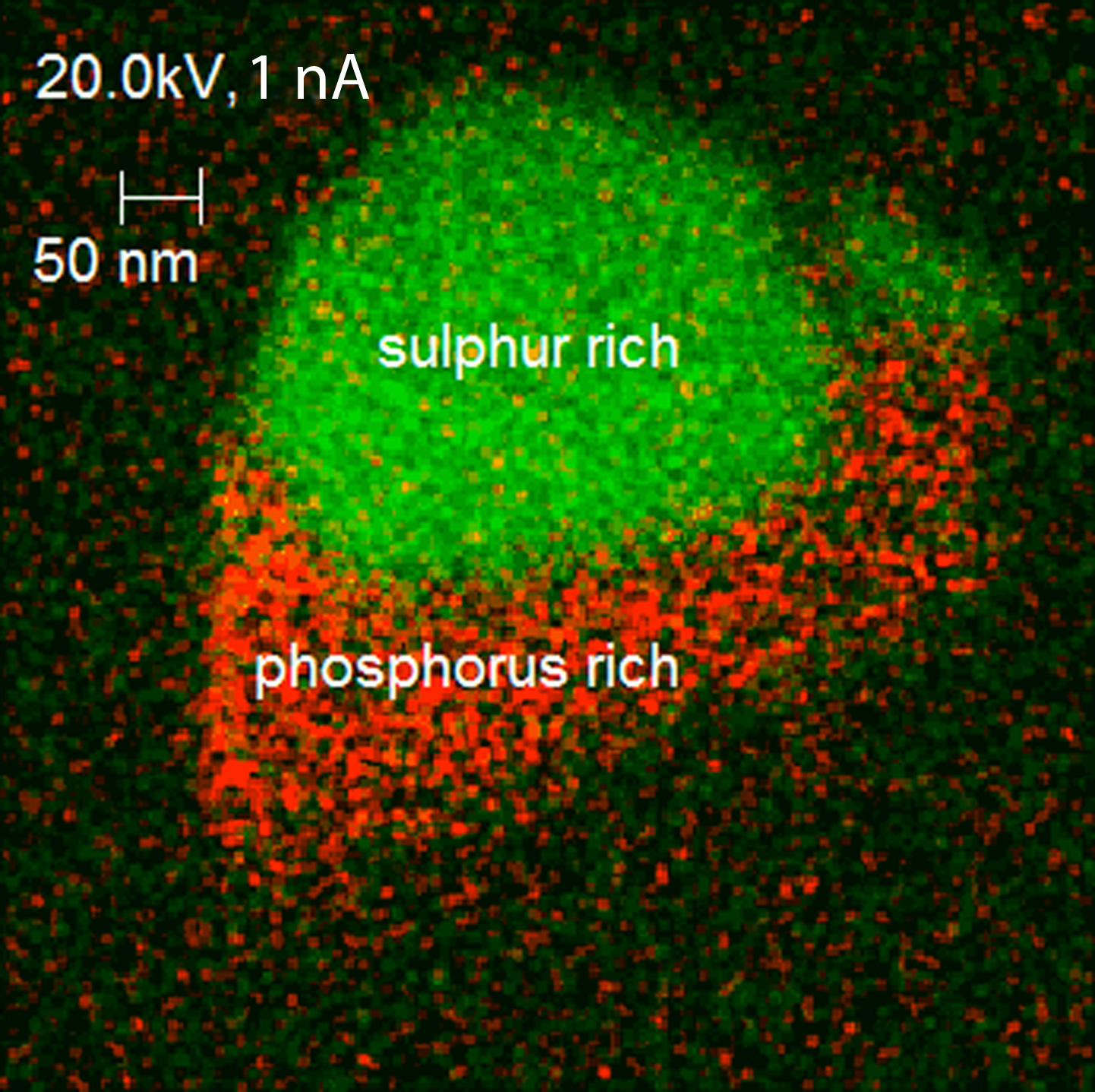
Image 2 shows a magnesium particle, roughly 400 nm x 400 nm large, that shows two distinctly different regions. The green colored areas are sulfur rich, while in the red areas phophorous is mixed with the magnesium.
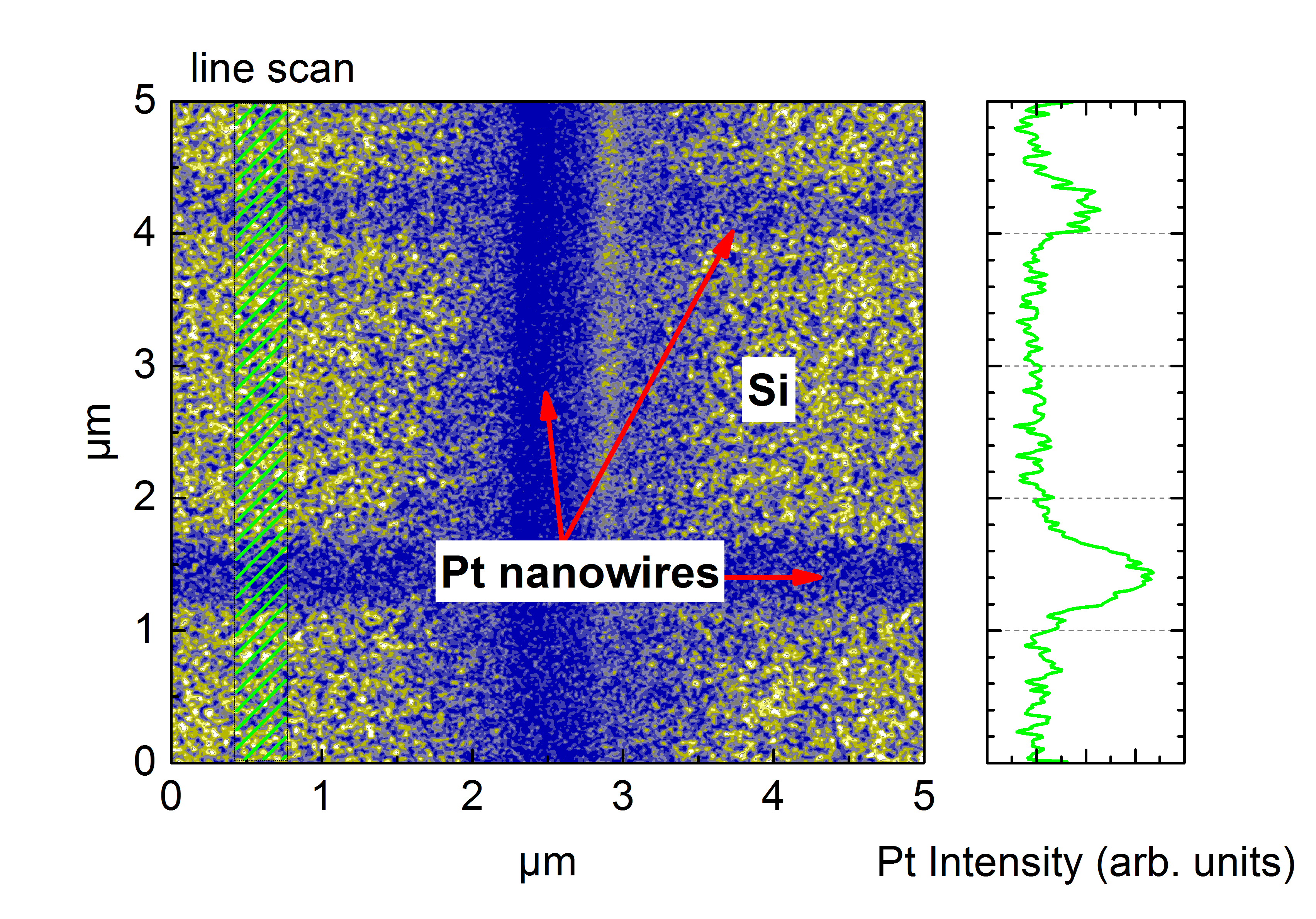
Platinum nanowires are shown in figure 3 (height 20 nm, 50 nm (width)), which were prepared onto a silicon substrate in the FIB. The auger signals of platinum (blue) and silicon (yellow) overlayed. The graph on the right gives the Pt-intensity along a line scan, represented by the green shaded area in the 2D map.
Scanning electron microscopy
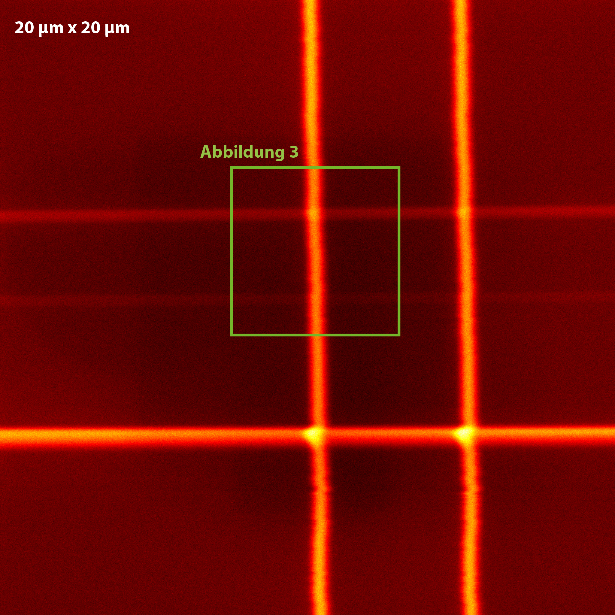
Due to the highly focussed electron beam it is possible to record secondary electron images (SEM). The NanoProbe 710 detects the generated seondary electrons using a scintillator detector. Figure 4 shows a 20 µm x 20 µm SEM image of platinum nanowires on silicon. The green rectangle depicts the area mapped as a chemical map in figure 3 (rotated by 180°).
Auger electron spectroscopy
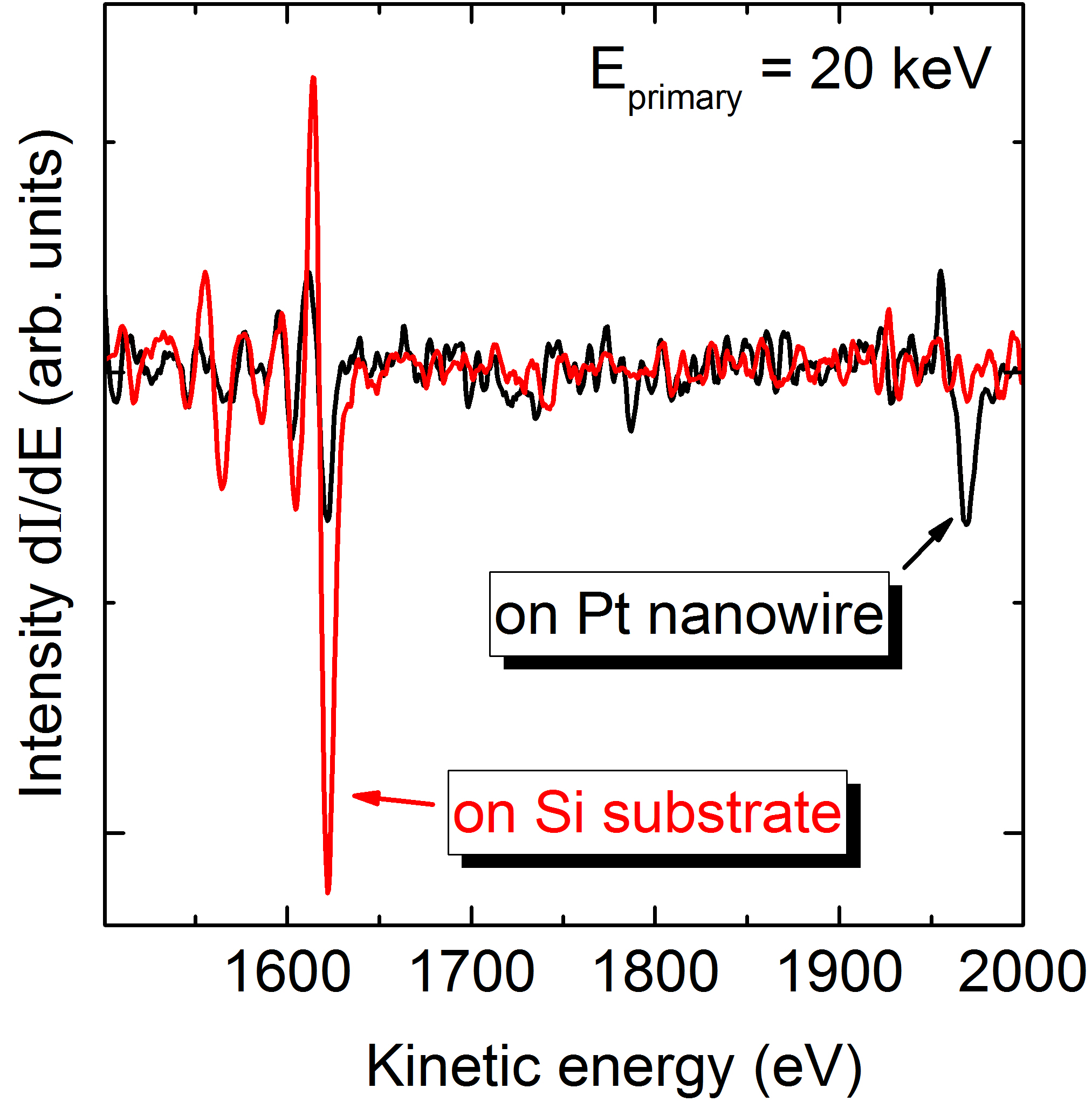
Figure 5 give the intensity dI/dE of the auger electrons in the kinetic energy range between 1500 eV and 2000 eV. This is, where peaks from silicon and platinum show up, which were used in generating figure 3. The red graph was recorded on silicon, the black one on the edge of a platinum nanowire. The signals from silicon and platinum, ca. 1622 eV, and platinum, ca. 1970 eV, are clearly visible.
![]()

Please contact:

Dr. Ulrich Hagemann (XPS, SAM, SIMS)
NETZ
Carl-Benz-Str. 199
47047 Duisburg
Room U1.15
Tel.: 0203 379-8035
E-Mail: ulrich.hagemann@uni-due.de
