

Photoelectron spectroscopy
What is photoelectron spectroscopy?
Photoelectron spectroscopy allows the determination of the elemental composition of a surface. It can distinguish between different elements as well as determine their precise bonding states. E.g. the signal of a carbon atom in a C-C bond differs from that of a carbon atom in a C-O bond.
The method is based on the detection of photoelectrons, emitted from the investigated surface under the illumination of (monochromatic) x-rays. One can distinguish between X-ray photoelectron spectroscopy (XPS, hν > 100 eV) and ultraviolett photoelectron spectroscopy (XPS, hν < 100 eV). The latter can be used to investigate the valence band of surfaces and molecular orbital energies.
The ICAN uses primarily a Versaprobe IITM by ULVAC-Phi. It offers a small minimal beam size of < 10 µm with a spectral resolution of 0.5 eV. Additionally x-ray induced electron imaging (SXI) allows for the in-situ imaging on the µm scale.
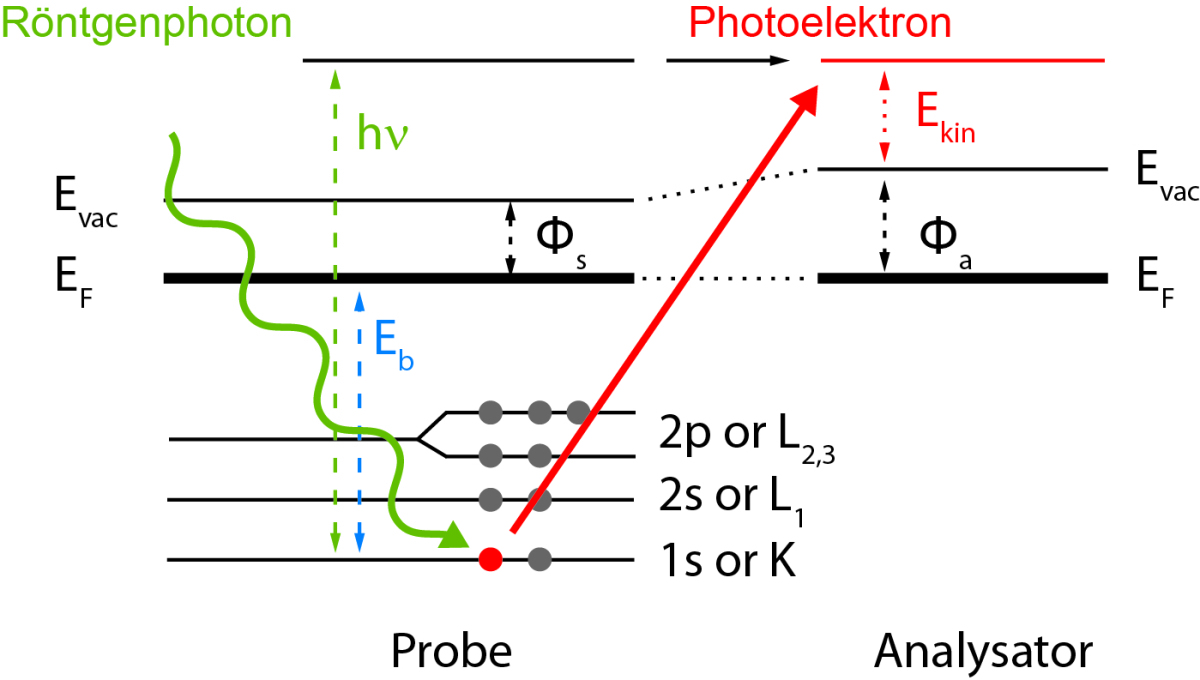
Figure 1: Schematic diagram of the excitation process in photoelectron spectroscopy. A x-ray photon an electron from a core-shell of the atom (here 1s). The photon energy is converted into kinetic energy of the electron, which is emitted into vacuum. Knowing the photon energy and measuring the kinetic energy of the electron then allows for determination of the binding energy of the electron.
Chemical analysis
The kinetic energy of the emitted electron depends on the element from which it originates, as well as from the precise bonding state of that atom. Picking up the carbon example from above, an electron from a carbon 1s shell has ~3eV kinetic energy less, if the atom is in a C=O double bon, rather than a in a C-C single bond.
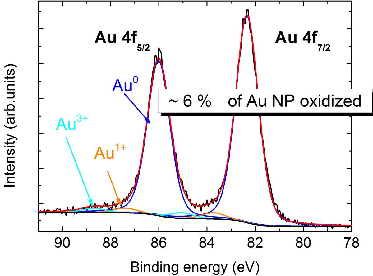
In figure 2 the Au 4f signal of a thin layer of gold nanoparticles is shown. A precise analysis yields, that roughly 6% of the gold atoms in the particles are oxidized, either as Au1+ or Au3+.
Figure 2: Intensity of the Au 4f peak of a thin gold nanoparticle layer. Small amounts of the gold is oxidized, which is why to additional peaks, representing the Au1+ (orange) and Au3+ (cyan) states are needed to describe the data.
Illustrations using SXI
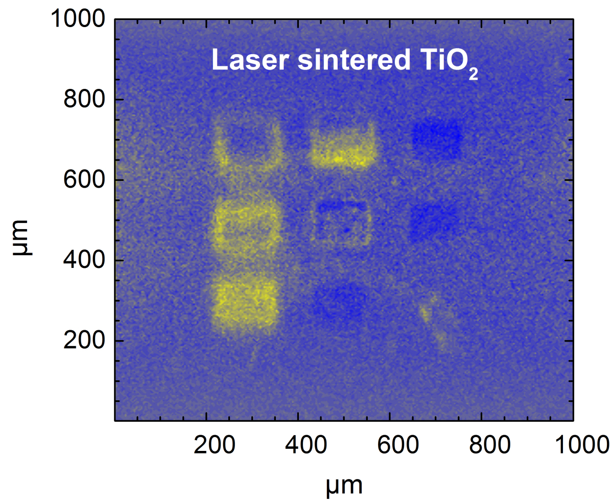
The following graph shows the detected X-ray induced secondary electrons (SXI) of a partially laser sintered TiO2 nanoparticle surface.
A laser was fired at the surface at 9 locations, varying the power of the laser. The variation of the laser power leads to a different degree of sintering of the TiO2 particles and thus to a different colour contrast.
Figure 3: An SXI of a laser-sintered TiO2 surface. The sintered surfaces are clearly visible.
Depth profiles and sputtering
With the existing system, it is possible to remove the surface of the sample to be examined by sputtering with argon ions.
On the one hand, this serves to clean the surface, as shown in Figure 4. By sputtering step by step, the antimony oxide layer that has formed on the surface of the sample is removed, leaving a pure, unoxidised antimony layer.
Furthermore, depth profiles can be recorded. After each sputtering step, the XPS intensity of the signal of the elements under investigation is determined. If the sputtering rate is known, the change in element concentration with increasing sample depth can be determined. An example is shown in Figure 5. It shows the intensity of Bi,Sb and Te of a BiSbTe3 layer as a function of the sputtering time. In this case, it can be seen that the concentration of tellurium and antimony decreases slightly with increasing depth.
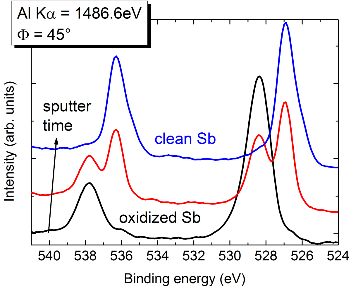
Figure 4: Change of the Sb 3d signal with an oxidised Sb surface and stepwise cleaning by sputtering with Ar ions.
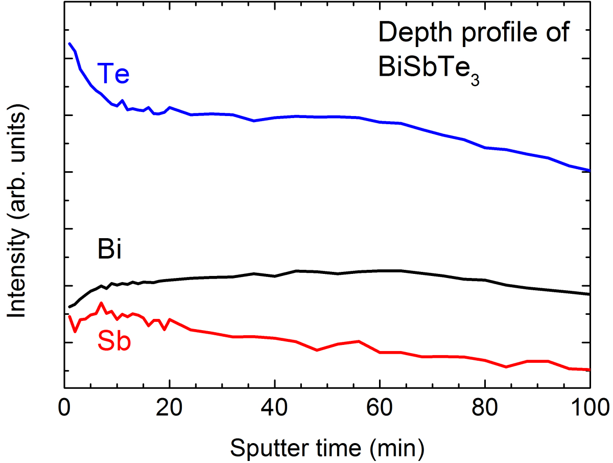
Figure 5: Depth profile of the intensity of the Sb, Te and Bi signal of a BiSbTe3 surface. By gradually removing the surface and measuring the signal intensity, a change in the composition of the layer can be detected.
2D chemical maps
With the help of the high spatial resolution of the X-ray beam, it is possible to record 2-dimensional maps of the chemical composition of a surface.
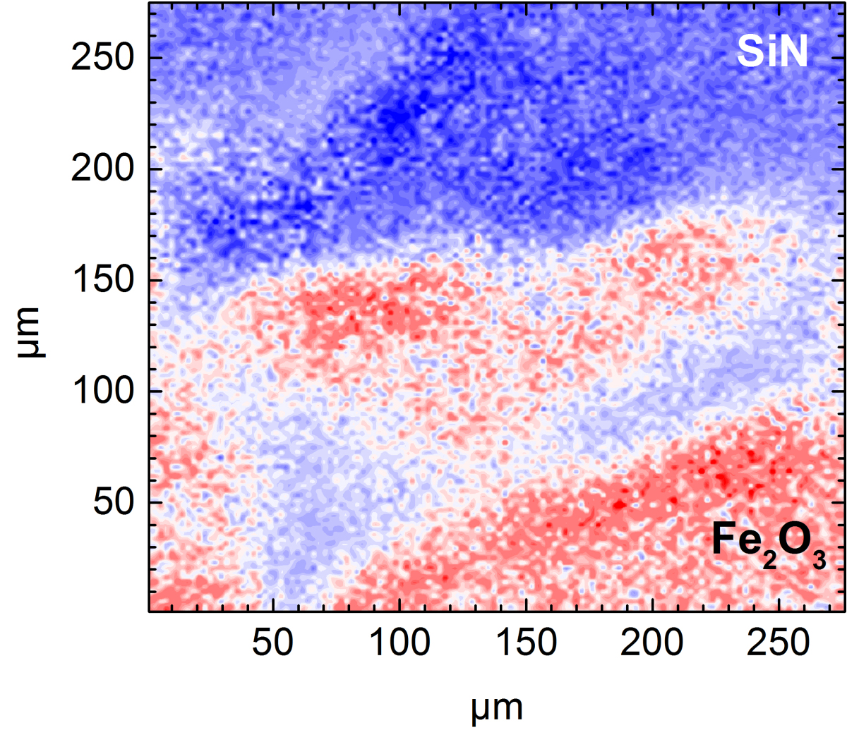
Figure 6 shows an example of this. Iron oxide and silicon nitride particles were applied to the sample as powder and measured. An area of just under 0.075 mm2 is shown. The intensity of the particles is colour-coded. The red areas show the iron oxide, while the blue areas represent silicon nitride.
Figure 6: Chemical map of Fe2O3 and SiN nanoparticles. The red coloured areas consist only of Fe2O3, the blue ones of SiN.
Surface and Quantum Well States
The high spectral resolution of He I light, depending on the system under investigation, combined with the smallest possible acceptance angle, enables the measurement of surface and quantum well states.
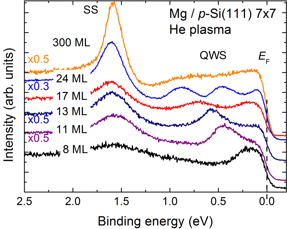
Figure 7 shows the monolayer dependence of these states of a crystalline magnesium layer on silicon. Depending on the layer thickness, one or more quantum well states and the increasingly sharp surface state can be seen.
Figure 7: UPS measurement of the surface state and quantum well states of a thin crystalline magnesium layer.
Determination of the work function
With the UPS it is possible to determine the work function of a surface. This is especially possible for metallic samples that have a non-vanishing electronic density of states at the Fermi energy.
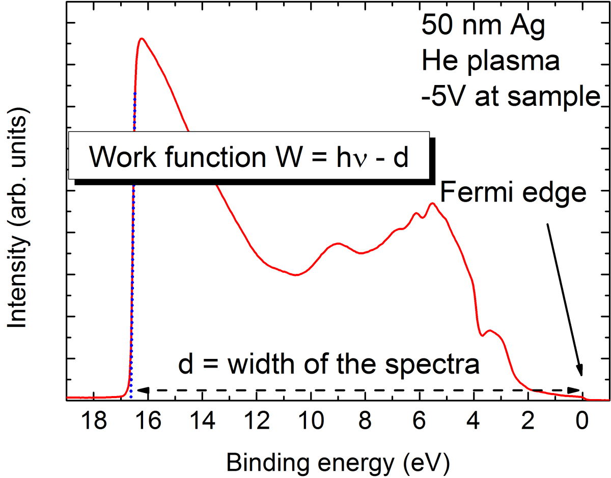
For this purpose, the width of the spectrum, i.e. the energetic distance between the insertion and Fermi edges, must be determined as precisely as possible. The work function of the surface to be examined then results from the difference between the photon energy and the width of the spectrum. In the example in Figure 8, a work function of 4.4 eV results for a 50 nm thick silver film on glass.
Figure 8: Determination of the work function of a 50 nm thick silver film on glass. The work function results from the difference between the photon energy and the width of the spectrum between the input and Fermi edges.
Your contact for XPS:
ICAN - Interdisciplinary Center for Analytics on the Nanoscale
47057 Duisburg
Functions
-
Wissenschaftliche/r Mitarbeiter/in, Center for Nanointegration Duisburg-Essen
Current lectures
No current lectures.
Past lectures (max. 10)
No past lectures.
The following publications are listed in the online university bibliography of the University of Duisburg-Essen. Further information may also be found on the person's personal web pages.
-
Anomalous Sub-Band Gap Emission at Room Temperature in Mixed-Dimensional WS₂/Cu₂O HeterostructuresIn: Small, 2026, in pressDOI (Open Access)
-
Designing 3D-Printed TiO2/BiFeO3-Hybrid Materials for Enhanced Photocatalytic Degradation of Acyclovir via Visible LightIn: ACS Applied Materials & Interfaces, Vol. 18, 2026, Nr. 19, pp. 27412 – 27425
-
Generation of hierarchical N-doped porous carbons from textile fabrics based on acrylic/wool fiber mixturesIn: Surfaces and Interfaces, Vol. 87, 2026, 108837DOI (Open Access)
-
Intrinsic activity and mechanistic insights in LaCoO₃ OER catalysts induced by support materialIn: Electrochimica Acta, Vol. 549, 2026, 147874DOI (Open Access)
-
Laser-Induced Iron Doping of Spinel Thin Film Electrocatalyst : Impact of Pulsed Laser Processing on Surface Cobalt Oxide Doping and Oxygen Evolution Reaction ActivityIn: ChemCatChem, Vol. 18, 2026, Nr. 2, e01233DOI (Open Access)
-
Mechanistic Understanding of Laser-Induced Defect Engineering of Anisotropic Cobalt Oxide Spinel Platelets in WaterIn: ChemCatChem, Vol. 18, 2026, Nr. 1, e01054DOI (Open Access)
-
Structural Characterization of Carbon-Doped and Carbon-Coated TiO₂ Core–Shell NanoparticlesIn: Advanced Materials Interfaces, Vol. 13, 2026, Nr. 2, e00770DOI (Open Access)
-
Tuning the oxygen evolution reaction activity of Co₃O₄ nanocubes via controlled metal doping and surface facetingIn: Chemical Engineering Journal, Vol. 537, 2026, 176110DOI (Open Access)
-
Ultra-Low Amounts of Transition Metals in Carbon-Based Catalysts Improve Their Alkaline OER Performance : A Systematic StudyIn: ACS Catalysis, Vol. 16, 2026, Nr. 15, pp. 14729 – 14749DOI (Open Access)
-
Understanding compositionally complex electrocatalysts using epitaxial films and correlative multi-scale characterization for structure–activity mappingIn: Materials Horizons, 2026, in pressDOI (Open Access)
-
Why and How Poly(acrylic Acid) Stabilizes and Structures Si/C Supraparticles for Li‐Ion Batteries : Unraveling PAA–Si/C Interactions From Dispersion to Electrode IntegrationIn: ChemElectroChem, Vol. 13, 2026, Nr. 10, e202600010DOI (Open Access)
-
ZnO Surface Morphology and Chemistry Govern Exciton Dynamics in WS2/ZnO HeterostructuresIn: ACS Applied Electronic Materials, 2026, in press
-
Conversion of acrylic/wool fibers to N-doped carbon materials for adsorption and electrochemical oxygen reduction to hydrogen peroxideIn: Surfaces and Interfaces, Vol. 69, 2025, 106756DOI (Open Access)
-
Effects of Dynamic Surface Transformation on the Activity and Stability of Mixed Co-Mn Cubic Spinel Oxides in the Oxygen Evolution Reaction in Alkaline MediaIn: Advanced Energy Materials, Vol. 15, 2025, Nr. 8, 2403096DOI (Open Access)
-
Glycerol Electrooxidation at Structured Nickel Electrodes and the Effect of Geometry on the Selectivity of ProductIn: ChemElectroChem, Vol. 12, 2025, Nr. 17, 2500175 , in pressDOI (Open Access)
-
Insight into the formation of carbon-doped titanate nanotubesIn: Chemical Engineering Journal Advances, Vol. 24, 2025, 100898DOI (Open Access)
-
Mechanistic and Structural Insights into the Liquid-Phase Oxidation of Cyclohexane over LaCo₀.₇Fe₀.₃O₃ Perovskite NanoparticlesIn: ACS Catalysis, Vol. 15, 2025, pp. 12773 – 12789
-
Unveiling Surface Species Formed on Ni-Fe Spinel Oxides During the Oxygen Evolution Reaction at the Atomic ScaleIn: Advanced Science, Vol. 12, 2025, Nr. 25, 2501967DOI (Open Access)
-
Core-shell Co₃O₄@CoO Nanoparticles for Enhanced OER ActivityIn: ChemCatChem, Vol. 16, 2024, Nr. 6, e202301327DOI (Open Access)
-
Correlating atomic-scale structural and compositional details of Ca-doped LaCO₃ perovskite nanoparticles with activity and stability towards the oxygen evolution reactionIn: Journal of Catalysis, Vol. 438, 2024, 115697DOI (Open Access)
-
Electrochemical Insights into Hydrogen Peroxide Generation on Carbon Electrodes : Influence of Defects, Oxygen Functional Groups, and Alkali Metals in the ElectrolyteIn: ACS Catalysis, Vol. 14, 2024, Nr. 23, pp. 17675 – 17689DOI (Open Access)
-
FeNi nanoparticle-modified reduced graphene oxide as a durable electrocatalyst for oxygen evolutionIn: Journal of Catalysis, Vol. 439, 2024, 115771DOI (Open Access)
-
Polyacrylonitrile-based porous polymer spheres and their conversion to N-doped carbon materials for adsorption and electrocatalysisIn: Journal of Applied Polymer Science, Vol. 141, 2024, Nr. 22, e55438DOI (Open Access)
-
Revealing Dynamic Surface and Subsurface Reconstruction of High-Entropy Alloy Electrocatalysts during the Oxygen Evolution Reaction at the Atomic ScaleIn: ACS Catalysis, Vol. 14, 2024, Nr. 17, pp. 12704 – 12716
-
Tunable Syngas Formation at Industrially Relevant Current Densities via CO₂ Electroreduction and Hydrogen Evolution over Ni and Fe-derived Catalysts obtained via One-Step Pyrolysis of Polybenzoxazine Based CompositesIn: Small, Vol. 20, 2024, Nr. 23, 2305958DOI (Open Access)
-
Versatile synthesis of sub-10 nm sized metal-doped MₓCo₃−ₓO₄ nanoparticles and their electrocatalytic OER activityIn: Materials Advances, Vol. 5, 2024, Nr. 8, pp. 3482 – 3489DOI (Open Access)
-
Atomic-Scale Insights into Morphological, Structural, and Compositional Evolution of CoOOH during Oxygen Evolution ReactionIn: ACS Catalysis, Vol. 13, 2023, Nr. 2, pp. 1400 – 1411
-
Cobalt nickel boride as electrocatalyst for the oxidation of alcohols in alkaline mediaIn: JPhys Energy, Vol. 5, 2023, Nr. 2, 024005DOI (Open Access)
-
Interaction of 2-propanol with predominantly SrO- and TiO2-terminated SrTiO3(100) surfaces studied by vibrational sum frequency spectroscopyIn: Catalysis Science and Technology, Vol. 13, 2023, Nr. 17, pp. 4988 – 4995DOI (Open Access)
-
Linking Composition, Structure and Thickness of CoOOH layers to Oxygen Evolution Reaction Activity by Correlative MicroscopyIn: Angewandte Chemie International Edition, Vol. 62, 2023, Nr. 28, e202305982DOI (Open Access)
-
Microscale Combinatorial Libraries for the Discovery of High-Entropy MaterialsIn: Advanced Materials, Vol. 35, 2023, Nr. 9, 2207635DOI (Open Access)
-
N-Doped porous carbons obtained from chitosan and spent coffee as electrocatalysts with tuneable oxygen reduction reaction selectivity for H₂O₂ generationIn: RSC Advances, Vol. 13, 2023, Nr. 33, pp. 22777 – 22788DOI (Open Access)
-
NiFe₂O₄/biochar decorated porous polymer membranes for the flow-through photo-Fenton degradation of tetracyclineIn: Chemical Engineering Journal, Vol. 477, 2023, 147203DOI (Open Access)
-
Polymeric multi-composites with a tailored nickel microenvironment as catalytic flow-through membrane reactors for efficient p-nitrophenol degradationIn: Chemical Engineering Journal, Vol. 463, 2023, 142437
-
Preparation of N-doped carbon materials from cellulose:chitosan blends and their potential application in electrocatalytic oxygen reductionIn: Polymer Bulletin, Vol. 80, 2023, Nr. 7, pp. 7827 – 7845DOI (Open Access)
-
3D atomic-scale imaging of mixed Co-Fe spinel oxide nanoparticles during oxygen evolution reactionIn: Nature Communications, Vol. 13, 2022, Nr. 1, 179DOI (Open Access)
-
Beneficial Effects of Low Iron Contents on Cobalt‐Containing Spinel Catalysts in the Gas Phase 2‐Propanol OxidationIn: ChemCatChem, Vol. 14, 2022, Nr. 18, e202200472DOI (Open Access)
-
Mono-, Di-, and Tri-Valent Cation Doped BiFe₀.₉₅Mn₀.₀₅O₃ Nanoparticles : Ferroelectric PhotocatalystsIn: Advanced Functional Materials, Vol. 32, 2022, Nr. 43, 2207105DOI (Open Access)
-
Structure-Performance Relationship of LaFe₁₋ₓCoₓO₃ Electrocatalysts for Oxygen Evolution, Isopropanol Oxidation, and Glycerol OxidationIn: ChemElectroChem, Vol. 9, 2022, Nr. 4, e202200092DOI (Open Access)
-
Ultrafast transport-mediated homogenization of photoexcited electrons governs the softening of the A1g phonon in bismuthIn: Physical Review B, Vol. 106, 2022, Nr. 1, 014315DOI, Online Full Text (Open Access)
-
Direct Detection of Surface Species Formed on Iridium Electrocatalysts during the Oxygen Evolution ReactionIn: Angewandte Chemie International Edition, Vol. 60, 2021, Nr. 39, pp. 21396 – 21403DOI (Open Access)
-
Large-Area, Two-Dimensional MoS2 Exfoliated on Gold : Direct Experimental Access to the Metal–Semiconductor InterfaceIn: ACS Omega, Vol. 6, 2021, Nr. 24, pp. 15929 – 15939DOI, Online Full Text (Open Access)
-
Nanopatterning surfaces by grazing incidence swift heavy ion irradiationIn: Applied Surface Science, Vol. 541, 2021, pp. 148467DOI, Online Full Text (Open Access)
-
Segregation-Enhanced Epitaxy of Borophene on Ir(111) by Thermal Decomposition of BorazineIn: ACS Nano, Vol. 15, 2021, Nr. 4, pp. 7421 – 7429
-
Spray-Flame Synthesis of LaMnO₃₊δNanoparticles for Selective CO Oxidation (SELOX)In: Energy & Fuels, Vol. 35, 2021, Nr. 5, pp. 4367 – 4376
-
The Effect of Water on the 2-Propanol Oxidation Activity of Co-Substituted LaFe₁−CoₓO₃ PerovskitesIn: Chemistry - A European Journal, Vol. 27, 2021, Nr. 68: Special Issue: Contemporary Challenges in Catalysis, pp. 17127 – 17144DOI (Open Access)
-
The Roles of Composition and Mesostructure of Cobalt-Based Spinel Catalysts in Oxygen Evolution ReactionsIn: Chemistry - A European Journal, Vol. 27, 2021, Nr. 68, pp. 17038 – 17048DOI (Open Access)
-
A swift technique to hydrophobize graphene and increase its mechanical stability and charge carrier densityIn: npj 2D Materials and Applications, Vol. 4, 2020, Nr. 1, 11DOI (Open Access)
-
Corrigendum to ‘Strong converse magnetoelectric effect in (Ba,Ca)(Zr,Ti)O₃-NiFe₂O₄ multiferroics: A relationship between phase-connectivity and interface coupling’ (Acta Materialia (2018) 144 (305–313), (S1359645417309072), (10.1016/j.actamat.2017.10.048))In: Acta Materialia, Vol. 187, 2020, pp. 91 – 92
-
Cover Feature: Spray‐Flame‐Prepared LaCo1–xFexO3 Perovskite Nanoparticles as Active OER Catalysts : Influence of Fe Content and Low‐Temperature Heating (ChemElectroChem 12/2020)In: ChemElectroChem, Vol. 7, 2020, Nr. 12, pp. 2495 – 2495DOI (Open Access)
-
Effect of Mn and Ba Codoping on a Magnetic Spin Cycloid of Multiferroic Bismuth Ferrite NanoparticlesIn: Journal of Physical Chemistry C: Nanomaterials and Interfaces, Vol. 124, 2020, Nr. 40, pp. 22266 – 22277
-
Effect of the Size and Shape on the Electrocatalytic Activity of Co₃O₄Nanoparticles in the Oxygen Evolution ReactionIn: Inorganic Chemistry, Vol. 59, 2020, Nr. 14, pp. 10013 – 10024
-
One-step synthesis of carbon-supported electrocatalystsIn: Beilstein Journal of Nanotechnology, Vol. 11, 2020, pp. 1419 – 1431DOI (Open Access)
-
Spray-Flame-Prepared LaCo₁–ₓFeₓO₃ Perovskite Nanoparticles as Active OER Catalysts : Influence of Fe Content and Low-Temperature HeatingIn: ChemElectroChem, Vol. 7, 2020, Nr. 12, pp. 2564 – 2574DOI (Open Access)
-
The effect of metal-oxide incorporation on the morphology of carbon nanostructuresIn: Journal of Physics D: Applied Physics, Vol. 53, 2020, Nr. 14, pp. 145206DOI (Open Access)
-
Correction : Determining the role of redox-active materials during laser-induced water decompositionIn: Physical Chemistry, Chemical Physics (PCCP), Vol. 21, 2019, Nr. 43, pp. 24239DOI (Open Access)
-
Determining the role of redox-active materials during laser-induced water decompositionIn: Physical Chemistry, Chemical Physics (PCCP), Vol. 21, 2019, Nr. 34, pp. 18636 – 18651
-
Effects of selenization time and temperature on the growth of Cu₂ZnSnSe₄ thin films on a metal substrate for flexible solar cellsIn: Solar Energy, Vol. 178, 2019, pp. 142 – 149DOI, Online Full Text (Open Access)
-
Lead diffusion in CaTiO₃ : A combined study using Rutherford backscattering and TOF-SIMS for depth profiling to reveal the role of lattice strain in diffusion processesIn: American Mineralogist, Vol. 104, 2019, Nr. 4, pp. 557 – 568
-
Nanoscopic Porous Iridium/Iridium Dioxide Superstructures (15 nm) : Synthesis and Thermal Conversion by In Situ Transmission Electron MicroscopyIn: Chemistry - A European Journal, Vol. 25, 2019, Nr. 47, pp. 11048 – 11057DOI, Online Full Text (Open Access)
-
Platinum nanoparticles supported on reduced graphene oxide prepared in situ by a continuous one-step laser processIn: Applied Surface Science, Vol. 469, 2019, pp. 811 – 820
-
Process Development for Wet-Chemical Surface Functionalization of Gallium Arsenide Based NanowiresIn: Physica Status Solidi (B): Basic Solid State Physics, 2019, pp. 1800678
-
Solution NMR Spectroscopy with Isotope-Labeled Cysteine (¹³C and ¹⁵N) Reveals the Surface Structure of l -Cysteine-Coated Ultrasmall Gold Nanoparticles (1.8 nm)In: Langmuir, Vol. 35, 2019, Nr. 3, pp. 767 – 778
-
Measuring displacement currents during fabrication of Mg/Si Schottky diodes due to band-bending evolutionIn: Journal of Applied Physics, Vol. 124, 2018, Nr. 22, pp. 225302
-
Strong converse magnetoelectric effect in (Ba,Ca)(Zr,Ti)O3 - NiFe2O4 multiferroics : a relationship between phase-connectivity and interface couplingIn: Acta Materialia, Vol. 144, 2018, pp. 305 – 313
-
UV-light assisted patterned metallization of textile fabricsIn: Applied Surface Science, Vol. 436, 2018, pp. 1093 – 1103
-
Adjusting the catalytic properties of cobalt ferrite nanoparticles by pulsed laser fragmentation in water with defined energy doseIn: Scientific Reports, Vol. 7, 2017, Nr. 1, pp. 13161DOI, Online Full Text (Open Access)
-
Gradual modification of ITO particle's crystal structure and optical properties by pulsed UV laser irradiation in a free liquid jetIn: Dalton Transactions, Vol. 46, 2017, Nr. 18, pp. 6039 – 6048
-
Improving the zT value of thermoelectrics by nanostructuring : Tuning the nanoparticle morphology of Sb2Te3 by ionic liquidsIn: Dalton Transactions, Vol. 46, 2017, Nr. 3, pp. 656 – 668DOI, Online Full Text (Open Access)
-
Laser-induced surface activation of biocomposites for electroless metallizationIn: Surface and Coatings Technology, Vol. 311, 2017, pp. 104 – 112
-
Microanalysis of single-layer hexagonal boron nitride islands on Ir(111)In: Applied Surface Science, Vol. 420, 2017, pp. 504 – 510DOI, Online Full Text (Open Access)
-
Synthesis of Sb2Se3 and Bi2Se3 Nanoparticles in Ionic Liquids at Low Temperatures and Solid State Structure of [C4C1Im]3[BiCl6]In: Zeitschrift für Anorganische und Allgemeine Chemie (ZAAC), Vol. 643, 2017, Nr. 1, Special Issue: Reactions in Ionic Liquids, pp. 60 – 68DOI, Online Full Text (Open Access)
-
Water-free synthesis of ZnO quantum dots for application as an electron injection layer in light-emitting electrochemical cellsIn: Journal of Materials Chemistry C: Materials for Optical and Electronic Devices, Vol. 5, 2017, Nr. 9, pp. 2344 – 2351
-
In Situ Investigations of Laser-Generated Ligand-Free Platinum Nanoparticles by X-ray Absorption Spectroscopy : How Does the Immediate Environment Influence the Particle Surface?In: Langmuir, Vol. 32, 2016, Nr. 35, pp. 8793 – 8802
-
Molecular design for tailoring a single-source precursor for bismuth ferriteIn: Inorganic Chemistry, Vol. 55, 2016, Nr. 15, pp. 7542 – 7549DOI, Online Full Text (Open Access)
-
Resonant laser processing of nanoparticulate Au/TiO2 films on glass supports : Photothermal modification of a photocatalytic nanomaterialIn: Surface Science, Vol. 650, 2016, pp. 57 – 63
-
Synthesis of Bi2Te3 and (BixSb1−x)2Te3 nanoparticles using the novel IL [C4mim]3[Bi3I12]In: Dalton Transactions, Vol. 45, 2016, Nr. 39, pp. 15326 – 15335DOI, Online Full Text (Open Access)
-
Direct self-assembly of Fe2O3/reduced graphene oxide nanocomposite for high-performance lithium-ion batteryIn: Journal of Materials Chemistry A: Materials for Energy and Sustainability, Vol. 3, 2015, Nr. 21, pp. 11566 – 11574DOI (Open Access)
-
Surface plasmon coupled chemiluminescence during adsorption of oxygen on magnesium surfacesIn: The Journal of Chemical Physics (JCP), Vol. 143, 2015, Nr. 24, pp. 244703
-
Van der Waals epitaxial MOCVD-growth of (BixSb1-x)2Te3 (0In: Semiconductor Science and Technology, Vol. 30, 2015, Nr. 8, pp. 085021DOI, Online Full Text (Open Access)In situ non-DLVO stabilization of surfactant-free, plasmonic gold nanoparticles : effect of Hofmeister's anionsIn: Langmuir, Vol. 30, 2014, Nr. 15, pp. 4213 – 4222Quantum size effects in chemicurrent measurements during low-temperature oxidation of Mg(0001) epilayersIn: New Journal of Physics (NJP), Vol. 16, 2014, pp. 113035DOI (Open Access)Internal detection of surface plasmon coupled chemiluminescence during chlorination of potassium thin filmsIn: The Journal of Chemical Physics (JCP), Vol. 138, 2013, Nr. 3, pp. 034710-1 – 034710-6Low temperature diffusion of Li atoms into Si nanoparticles and surfacesIn: Journal of Applied Physics, Vol. 114, 2013, Nr. 3, 034310Electronic excitations generated by the deposition of Mg on Mg filmsIn: Physical Review Letters, Vol. 104, 2010, Nr. 2, pp. 028301Electronic excitations in magnesium epitaxy: Experiment and theoryIn: Physical Review B: Condensed matter and materials physics, Vol. 82, 2010, Nr. 15, 155420-1-9
Thesis
Quantum size effects in Mg epilayers on Si (111) : enhancement of photoelectron yield and oxidation rateDuisburg, Essen, 2015Research report
Focus Track – How to minimize and compensate z-Axis drift using the Renishaw InVia Raman microscope2021
(ICAN Notes)DOI, Online Full Text (Open Access)Lectures
Neue Erkenntnisse zur Keimbildung bei GJS
Österreichische Gießereitagung ; Gurten, 27.-28. April 2017,Gurten, Österreich, 2017