
Printable Materials for Signal Processing Systems
| |  Currently active group members:Prof. Dr.-Ing. Niels Benson |
|
|
The working group “Printable Materials for Signal Processing Systems” concentrates on “low-cost” electronic applications, in order to make the attribute “printable” attractive / applicable for signal processing systems. Such systems are especially interesting for industry 4.0 applications as well as the internet of things (IOT). In this effort the research of the group uses a holistic approach, starting with the elementary understanding of charge carrier transport related phenomena, and ending with application related questions. With respect to applications, the group goes beyond a single device type and covers devices ranging from components for signal processing, to components for energy storage and energy generation. This results into the following current research areas: New materials for signal processing systems.
Dispersed in organic solvents, Si nanoparticles are printable with common methods such as inkjet printing. Using a subsequent laser modification step, the nanoparticle thin film can be optimized with respect to its electronic functionality, in order to allow for printed electronic applications. One example under investigation in the Benson group are printable RFID tags. The main idea behind this work, is the combination of advantages typically associated with organic and metal oxide semiconductors, with the advantages of a classical semiconductor system. Consequently, the aim of this research is the development of a technology, which is not only printable and mechanically flexible (organic and metal oxide semiconductor systems), but also stable with a performance similar to classical semiconductors such as Si.
Additive ceramic manufacturing has an enormous potential for signal processing systems in the mm and sub-mm wavelength range, mainly because of the digital freedom of the 3D printing technology in combination with the obtainable material quality. These advantages play out especially nicely, when it comes to monolithic multicomponent integration, without the negative influence of assembly issues or intermodulation products. Currently, the work of the Benson group is concentrating on structure minimization in the sub 200µm range, the frequency dependent material evaluation, as well as the implementation of first applications. 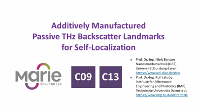 Video: Additive Manufacturing (AM) for signal processing applications
Energy storagethe research with respect to this topic is done in close cooperation with different industry partners, and mainly concentrates on the development of anode structures for battery applications. The main aim of this work is the improvement of the obtainable capacity, the charging speed and the security of batteries for IOT applications. For this purpose, different anode concepts using Si nanoparticle structures are evaluated. Here, the focus of the Benson group lies on the generation of the anode µ-structure, the modeling of the thin film formation using a fluidic finite element simulations, and the testing of appropriate half cells.
Energy generationthe work on energy generation for IOT applications is part of the holistic approach of the Benson group, covering applications ranging from electronic loads, to energy storage and generation. For the purpose of energy generation, the group does research on perovskite solar cells, which are potentially printable and allow for power conversion efficiencies of > 23% in thin film devices. Here, the group has achieved a good state of the art with Methylammonium Lead Iodide (MAPI) cells, reaching efficiency values of > 19%. Having achieved this milestone, the group is currently concentrating on the experimental evaluation of mainly theoretical postulates regarding the beneficial trap physics of perovskite thin films.
Novel methods for the charge carrier transport evaluationThe charge carrier transport properties of a material system mainly determine its possible applications. Consequently, research on this topic is an important part of the Benson group. In this framework we were able to introduce / improve the following two methods:
Classical TSC experiments use diode structures for the evaluation of a trap density of states distribution. This choice in device type has the disadvantage, that leakage currents and ambipolar injection (due to long measuring times of up to 1 week) negatively influence the measurement either by artefacts in the current signature or by recombination effects. Further, for the quasi-unipolar evaluation of a single charge carrier type, very different device architectures are required, which may strongly influence the data interpretation. This is why the Benson group has introduced a MIS structure for TSC experiments, allowing for unipolar evaluation of complementary charge carriers using one and the same device. For these experiments, the charge carrier in the device is defined by the polarity of the applied voltage.
The evaluation of the charge carrier mobility using the steady state SCLC approximation, is a wide spread method, which is often negatively influenced by the non-ideality of the device under investigation. By supplementing this technique using transient SCLC measurements on the same device, the steady state evaluation can be self consistently verified. For this purpose, a measurement circuit was designed allowing for extremely short RC time constants and a circuit oscillation suppression, which enables the measurement of device transit times in the range of 300ns. For thick devices structures in the range of 1µm, this enables the measurement of charge carrier mobilities up to 1cm2/Vs. |
We are responsible for the following start up project:  |
Third party funding:      |