
Bachelor-& Masterthesis


01.07.2024
Bachelor/Master thesis
Understanding Recombination Mechanism of Organic Solar Cells by Capacitance Measurements
Capacitance measurements allow the determination of recombination lifetimes and doping densities, which are important for understanding and quantifying the loss mechanisms of solar cells. In this project, we will fabricate organic solar cells using methods such as spin-coating and evaporation. We will then aim to correlate the process parameters used during device preparation with loss mechanisms quantified using capacitance measurements. During the master thesis, the student will
- Fabricate organic solar cells using a variety of different process parameters and perform capacitance measurements and light-intensity dependent current voltage curves.
- analyze the data and correlate process parameters, performance and the time constants obtained from capacitance measurements.
Machine Learning-assisted Optimization of Organic Solar Cells towards Thick (>250nm) Absorber Layers
From an industrial perspective, a thick (> 250 nm) absorber layer is necessary to successfully fabricate organic solar cells with a high yield in a roll-to-roll process. However, a device with thick active layer suffers from reduction in fill factor and efficiency since the charge carriers need to travel much longer to reach the contacts. In this project, we aim to produce devices with higher thickness which, nevertheless, retains high efficiency (>15%) with the help of a machine-learning assisted design of experiment approach. Furthermore, we aim to understand the loss mechanisms in the device.
- Design and conduct experiments on the fabrication of organic solar cells.
- Characterize device performance using various measurement techniques.
- Develop machine learning models to predict the performance of organic solar cells with thicker absorber layers.
We have outlined two potential projects; however, we are also open to collaboratively identifying an area of interest that aligns with the student's preferences and goals.
Contact email: e.kim@fz-juelich.de, l.christen@fz-juelich.de
07.02.2024
Hello everyone
There is a possibility of doing master's/bachelor's project and thesis in our group. The title is not yet finalized, but it related to the field of “3D printing of ceramic”. Please contact me (masoud.sakaki@uni-due.de) if you:
- Have a background in chemistry, materials science, or comparable areas.
- Have experience working in a laboratory.
- Can notice details and detect tiny imperfections.
- Are willing to learn new things.
- Can focus and investigate deeply.
- Have good computer skills and intermediate proficiency in English.
Best regards,
Sakaki
4.10.2021
Spraycoating of Silicon Nanoparticles as Anode Material in Solid State Batteries
The reasearch in our group about solid state batteries is carried out as part of the "OptiKeraLyt" project (material and process optimization for lithium-ion batteries with ceramic solid state electrolytes). Within our subproject, one of the issues is the connection between anode and solid state electrolyte. In particular we are investigating the spraycoating of planar and surface structured solid state electrolytes with silicon nanoparticle dispersions. Important parameters are the coating homogeneity and the achievable coating thicknesses and porosities.
Possible topics for Master/Bachelor theses and projects:
- Investigation of the silicon nanoparticle layer formation during spraycoating -> experimental investigation and model development
- Investigations into the reduction of so-called coffee ring structures (accumulation of nanoparticles at the droplet edge) by suitable choice of dispersing media
- Analysis of sprayed layers by means of light-, electron- and confocal-microscopy
- Experiments on the planarization of sprayed nanoparticle layers
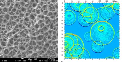
left: Scanning electron microscopy image of a spray coted silicon nanoparticle layer, right: confocal microscopy image of single spray coated silicon nanoparticle droplets
|
Contact: |
M.Sc. Julian Neises |
|
Email: |
4.10.2021
Additively manufactured ceramic parts
The novel LCM method (lithography-based ceramic manufacturing) can be used to additively manufacture ceramics such as alumina and zirconia. In this process, suspension thin films with a ceramic nanoparticle content of 40-65% are selectively crosslinked step by step using the DLP (Digital Light Processing) principle to form a 3D workpiece. In the subsequent step, a heat treatment is mandatory to burn out the crosslinked polymer and trigger a sintering process. The materials produced in this way are investigated in terms of their structural and electromagnetic properties.
Possible topics for Master/Bachelor theses and projects:
- Influence of printing and sintering parameters on microstructure and surface quality
- Investigation of printed and sintered structures using light, electron and confocal microscopy, profilometer measurements and determination of density/porosity
- Structured surface modification by laser-induced metallization
- Simulation and measurement of the electromagnetic properties of additively manufactured structures
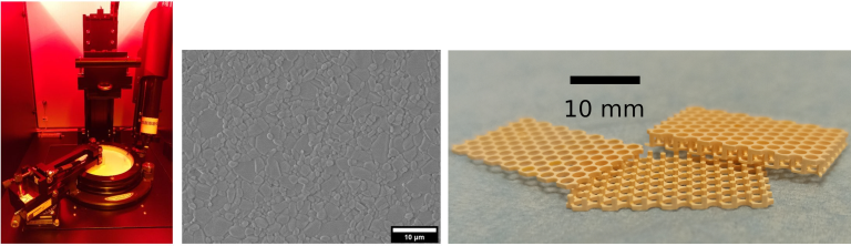
left: Setup of the 3D printer, middle: scanning electron microscope image of sintered alumina, right: examples of complicated structures that can be produced via LCM technique.
|
Contact: |
Dr. Masoud Sakaki |
|
Email: |
|
|
Contact: |
M.Sc. Kai-Daniel Jenkel |
|
Email: |
4.10.2021
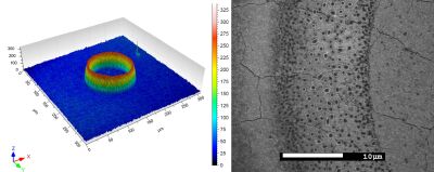
Lithium-Ion Battery Anodes based on Silicon Nanoparticles and vertically aligned Carbon Nanotubes
A new concept for silicon-based anodes with high rate capabilities is investigated. Vertically-aligned carbon nanotubes (CNT-forests/VACNTs) grown via chemical vapor deposition act as electrically conductive scaffolding with the aim to expand the two-dimensional surface of Cu current collectors. Silicon nanoparticles (Si-NP) integrated into this CNT-structure are used as active material due to their high Li storage capability and their high tolerance against pulverization. Compared to conventional anodes, this concept offers a higher proportion of active material in direct electrical contact with the current collector and hence, possibly better performance at higher current densities. Figure 1 b) illustrates the basic anode concept. As grown VACNTs are densely packed and therefore, leave no space for a coating with Si-NPs beyond the topmost surface (Fig. 1 a) & c)). In order to be able to benefit from the CNT’s advantages, two methods for structuring VACNTs were developed: UV-Laser and solvent treatment. These process steps induce a “CNT-bunching” which yields a compacted structure with gaps that can be used for the infiltration of Si-NPs (Fig. 1 b) & d)). Si-NP deposition is achieved via doctor blading, spray coating and dip coating
Master/Bachelor theses and projects typically include the following fields of work:
- Anode manufacturing via doctor blading, spray coating and dip coating.
- SEM analysis of samples.
- Assembly of electrochemical test cells/batteries.
- Electrochemical measurements, such as galvanostatic/potentiostatic cycling, electrochemical impedance spectroscopy, cyclic voltammetry.
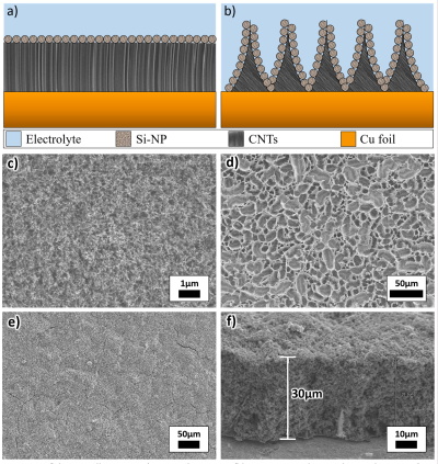
Schematic illustration of our anode concept. Silicon nanoparticles (Si-NP) are deposited on top of an electrically conductive scaffold of vertically aligned carbon nanotubes (VACNTs). a) as grown VACNTs leave no space for Si-NP infiltration; b) structured VACNTs provide side walls that can be covered with Si-NP. Top view SEM image of a VACNT layer: c) untreated; d) after ethanol spray treatment. SEM image of a VACNT layer after slurry deposition via dip coating: e) top view, f) cross-sectional view, the voids between CNT-bunches are now completely fill with anode active material (Si-NP)
|
Contact: |
M.Sc. Damian Pandel |
|
Email: |
4.10.2021
Inkjet-printed Silicon Schottky diodes
By dispersing silicon nanoparticles in suitable organic solvents, Silicon is made printable. Inkjet printing enables the deposition of single droplets in the picoliter range, that can subsequently be functionalized by laser treatment and be utilized to produce Schottky diodes. By developing specialized Silicon inks and thereby controlling the drying behaviour, fine patterning of the deposited nanoparticles - even below the native resolution of inkjet printing - can be achieved.
Possible topics for Master/Bachelor theses and projects:
- Inkjet-printing of dispersed Silicon nanoparticles, foto resist and metal inks
- Development of Silicon inks for optimisation of nanoparticle deposition profiles
- Investigation of printed nanoparticle structures by light, electron and confocal microscopy; profilometer measurements and UV excimer laser treatment
- Fabrication of Schottky diodes and electrical characterisation thereof by measurements of IV characterstics and high frequency operation
Left: Threedimension confocal image of an inkjet-printed Silicon nanoparticle structure. Right: Scanning electron microscope image of the nanoparticles after structuring by laser treatment
|
Contact: |
M.Sc. Fabian Langer |
|
Email: |
4.10.2021
Fabrication, characterization and optimization of Silicon µ-cone Schottky diodes
The laser treatment of a Si nanoparticle thin film results in a self-organized cone-shaped μ-structure (µ-cones), which is highly crystalline. Sandwiched between two metal layers, whereby one is forming a Schottky contact to the Si µ-cones, Schottky diodes with switching speeds in the GHz-range can be realized. Due to the lateral discontinuity of the μ-cones, as well as their small footprint, this structure is expected to be mechanically flexible.
In this context, the following topics are of interest for future graduate work:
- The realization of µ-cone Schottky diodes on flexible substrates such as paper or foils
To demonstrate the flexibility of the µ-cone Schottky diodes, the transfer of the diode structure to flexible substrates is needed.
- The reduction of losses due to parasitic current paths by integrating a printing process for Si-NP deposition
So far, the diode functionality of the µ-cone Schottky diodes could be demonstrated up to 4GHz, although this measurement is limited due to relatively high losses. The aim is therefore to reduce these losses, for example by reducing parasitic current paths by integrating a printing process for the Si-NP deposition.
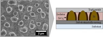
left: Scanning electron microscope (SEM) image of self-organized cone shaped Si structure caused by the laser treatment of a silicon nanoparticle thin film (top view); right: schematic image of the diode structure (side view)
|
Contact: |
M.Sc. Laura Kühnel |
|
Email: |
15.11.2022
Probing of perovskites with regard of charge carrier trap states
In the past years materials, which crystallise in the so called perovskite structure in an ABX3 schematic, have gained a lot of interest in the scientific community regarding optoelectronic applications. By using them solar cells on lab level with power conversion efficiencies (PCE) up to 25,7 % could be realised. This is around the PCE of the heavily researched, expensive silicon technology (PCE 26,1 %). The greatest hurdles for a commercialisation of the perovskite technology lay on the one hand in the big risk for both health and environment due to lead being incorporated in perovskites used for highly efficient solar cells, and on the other hand in the high level of degradation of these perovskites triggered by environmental influences such as humidity or temperature To tackle both problems lead can be substituted by comparable elements, which however leads to cells with PCEs well below the record values. A possible explanation for bad efficiencies could be so called trap states within the perovskites, which would be the origin of stronger recombination effects and by that lower the extractable current. To characterise these states thermally stimulated currents (TSC) in unipolar setups from metal, insulator and semiconductor (MIS) in the so-called MIS-TSC can be utilised, which would allow to assign specific energy levels to the trap states.
Possible topics for a Bachelor`s or Master’s thesis and project work:
- Optimisation of thin films for the MIS-TSC
- Characterisation of suitable Contact materials
- Comparison of trap distributions in films from different methods of synthesis
- Comparison of trap distributions in thin films and single crystals
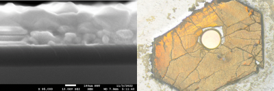
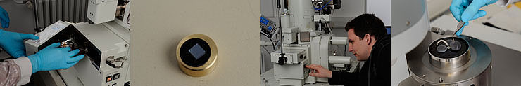
Left: Cross section picture via scanning electron microscopy of a MAPbI3 thin film on a Si- SiO2 substrate, right: Single crystal of a CsAgBiBr6 perovskite
|
Contact: |
M.Sc. Lars Leander Schaberg |
|
Email: |
Further topics, please contact: Andreas Trampe
However, you can also address all scientific staff in the NST department to specific questions that are of particular interest to you.