
Lab Equipment
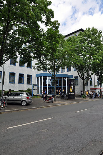 |
Location DuisburgThe laboratories of the Department of Nanostructure Technology are located on the second and third floors of the BA building on Bismarckstraße in Duisburg. On a laboratory area of more than 450 m², more than 20 scientists are currently working on the development of new functional layers and devices. A selection of some of the measuring equipment and methods is shown below. |
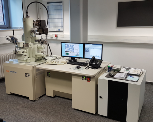
JEOL JSM-7500F high resolution field emission scanning electron microscope
|
 |
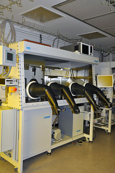 |
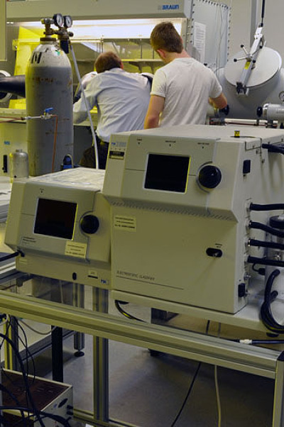
Nitrogen glovebox (MB 200 B, MBRAUN)A glove box is an area that is hermetically sealed and gas-tight to the surrounding laboratory. A defined atmosphere is maintained inside, consisting of inert gases such as nitrogen (or argon). A glove box is used to protect samples and materials from reacting with oxygen or water from the laboratory air.
|
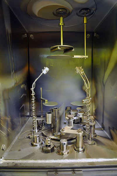
Vacuum evaporation systemThis evaporation system is a high vacuum system. It is used to deposit materials (metals, dielectrics, semiconductors) onto substrates. The evaporation process takes place in a high vacuum. |
 |
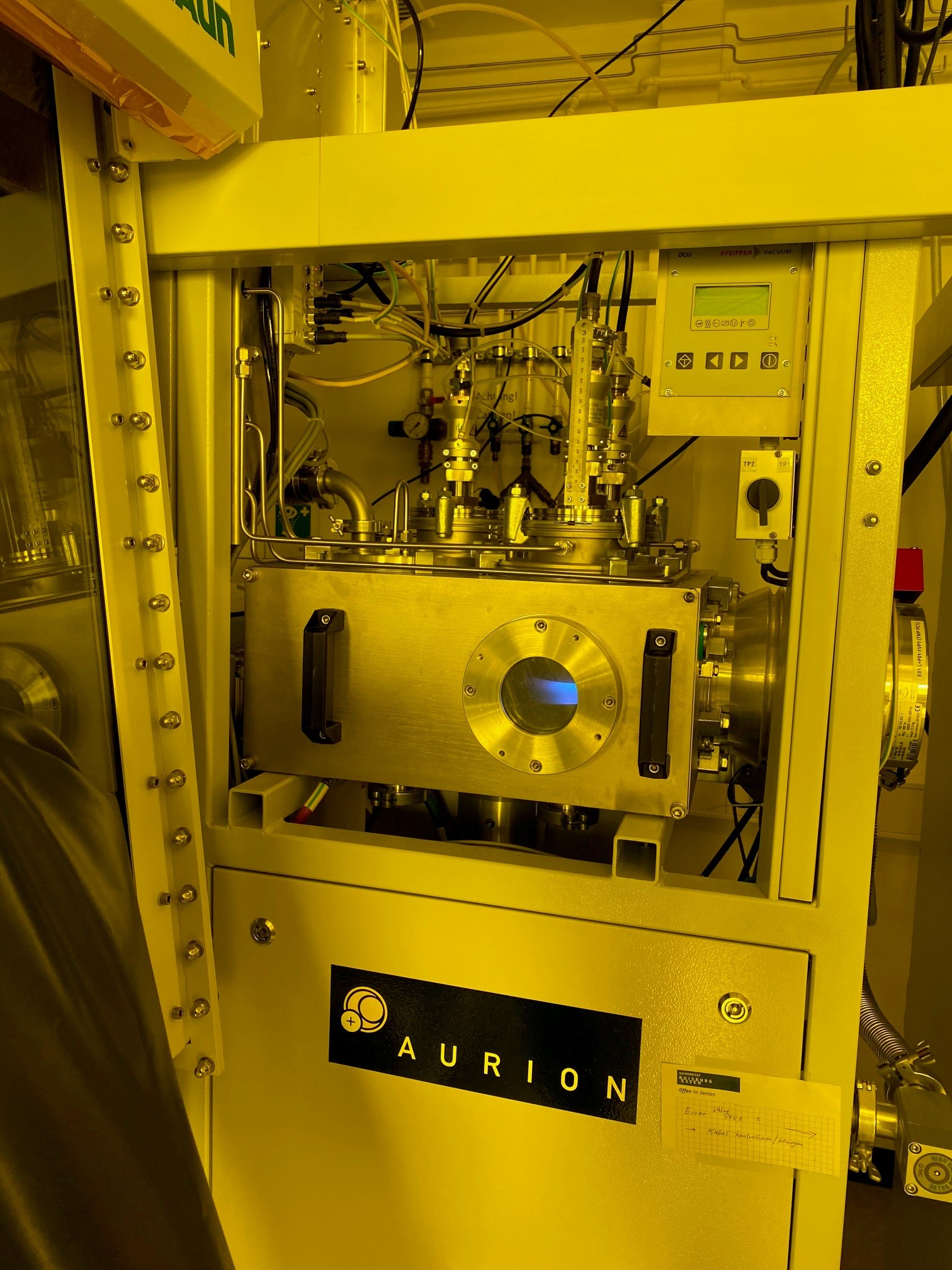 |
Magnetron Sputter Cluster Facility, Aurion AnlagentechnikThis facility utilizes the sputtering principle to coat substrates with metals, semiconductors or insulators. Ar atoms are ionized and accelerated towards a solid state target, where their kinetic energy leads to a removal of target atoms, that are subsequently deposited onto the substrate, producing homogeneous thin films in nanometer to micrometer range. By reactive ion etching, different materials such as photoresists can be etched. |
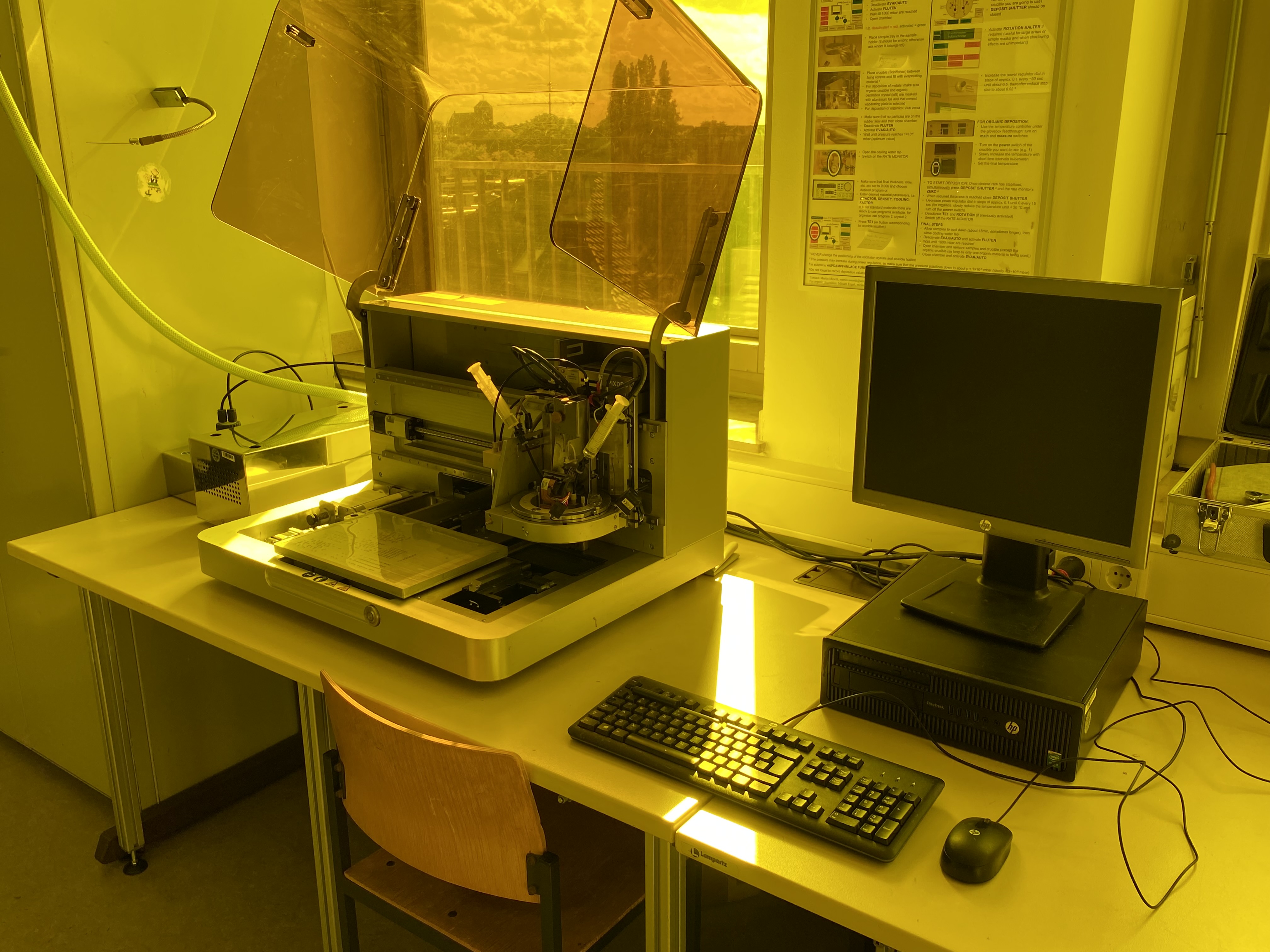
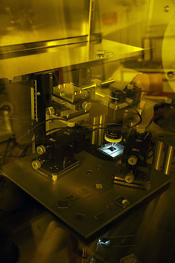
Pulsed KrF-Excimer Laser ATLEX-300SI, ATL Lasertechnik GmbHThe short pulse excimer laser ATLEX-300SI is a compact, air cooled UV-laser. For the sample processing it is integrated into an overall system of Lissotschenko Mikrooptik GmbH (LIMO). Both the focus (z-axis) and the processing area in the x-y plane can be adjusted via a traversing unit and can be controlled during the laser process. In our groupt it is used to laser modify silicon nanoparticle (Si-NP) thin films, leading to a self-organized formation of crystalline μ-cone shaped structures. Technical Data |
 |
 |
Inkjet printer PiXDRO LP50, Meyer BurgerThe PiXDRO LP50 allows for micrometer-precise deposition of functional materials. To accommodate inks with different rheological and chemical properties, a series of print heads can be installed, enabling the deposition of varying materials, for example dispersions of metallic or semiconducting nanoparticles, starting at only a few picolitres (10-12 litres). |
Semiconductor characterization systemFour-probe measurement system with system-source meter unit (SMU) Keithley 2612. Keithley 4200-SCS with Four-probe measurement system
|
 |
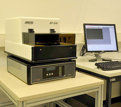 |
Profilometer (XP-200 High Resolution Stylus-Type Surface Profilometer, Ambios Technologies)A profilometer can be used to determine topographies of specimen surfaces at the microscopic level. For this purpose, a thin diamond tip is dragged over the sample on a lever arm in contact mode. The deflection of the lever arm is detected by a laser beam. The deflection can be used to infer the roughness of the sample surface. When measuring edges, layer thicknesses can also be determined.
|
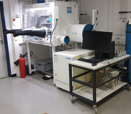
Ar-Glovebox und battery test systemsLeft Side: MBraun "UNIlab pro" Glovebox with Argon atmosphere for the manufacturing of batteries/electrochemical test cells and for the storage of battery components, such as Lithium, electrolyte, cathode and anode materials. Right Side: Measurement setup for batteries/electrochemical test cells consisting of a PAT-Tester-x-8 (EL-CELL) and a BTS-4000 test system (NEWARE). |
 |
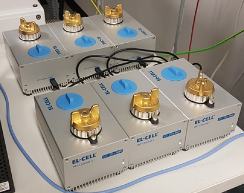 |
PAT-Tester-x-8 by EL-CELL with six test channels
|
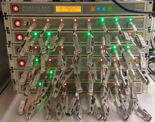
BTS-4000 test system by NEWARE with 48 test channels
|
 |
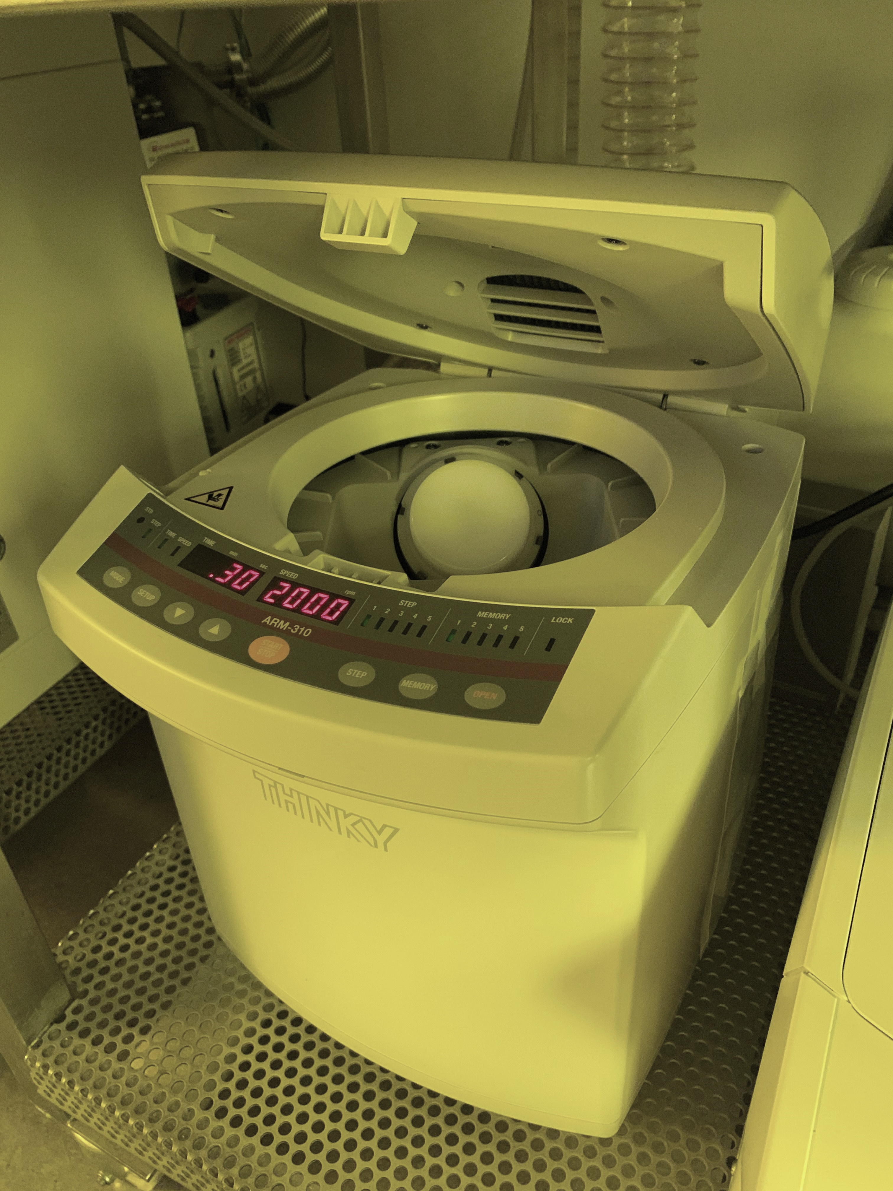 |
ARM-310 Planetary Centrifugal Mixer, Thinky Corporation
The ARM-310 planetary centrifugal mixer enables mixing of various components without a stirrer. Highly efficient mixing is achieved by a superposition of centrifugal and self-rotating motion. The acting centrifugal forces result in an effective degassing of the mixture. The ARM-310 is used by us for the production of highly viscous battery slurries for silicon-based anodes in lithium-ion batteries. |
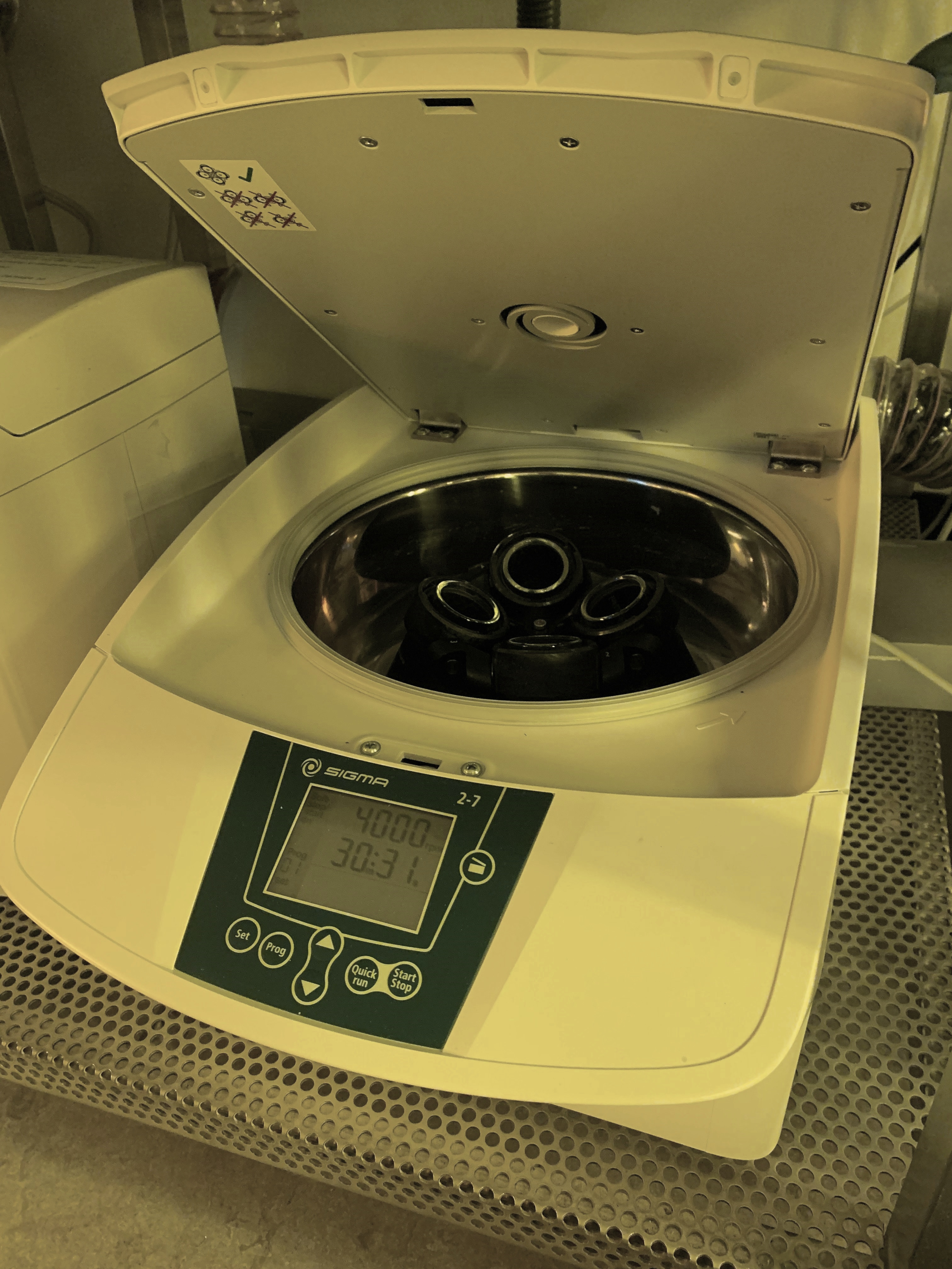
Benchtop centrifuge Sigma 2-7, Sigma Laborzentrifugen GmbHCentrifuges can be used to separate components of dispersions and emulsions by utilizing centrifugal force. Max. Speed: 4000 min-1 |
 |
 |
LFA 457 Microflash, NETZSCH-Gerätebau GmbHThe NETZSCH LFA Microflash 457 can be used to determine the thermal conductivity of materials. This is a non-contact, transient measurement method. A short infrared laser pulse is used to heat the front side of the sample under investigation, while the temperature development on the back side of the sample is recorded as a function of time using a liquid nitrogen-cooled infrared radiation detector. Thermal diffusivity and specific heat capacity (reference sample required) can be determined from the time-resolved temperature profile. These material parameters can be used, together with the density, to infer the thermal conductivity. The sample is coated on both sides with graphite for uniform absorption and emission of the laser radiation. Up to 3 samples can be measured simultaneously in a temperature range from 25°C to 1000°C. Available measuring atmospheres: Nitrogen, argon, 5% hydrogen in argon, helium, synthetic air. |
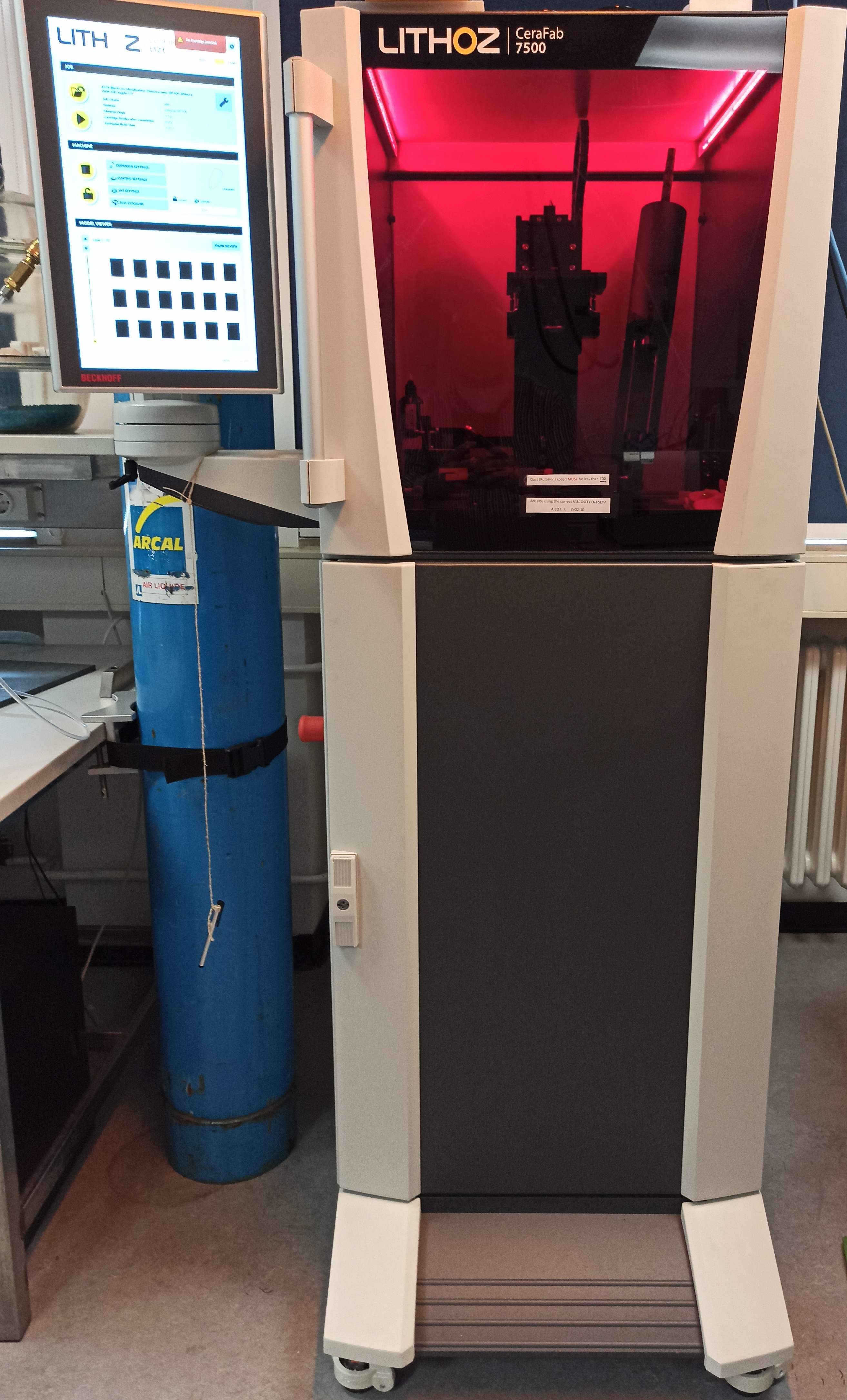
3D-Drucker (LITHOZ-CeraFab 7500)CeraFab 7500 is a lithography-based 3D printer. During the printing, a thin film of ceramic suspension is selectively cross-linked by a UV source using DLP (Digital Light Processing) principle to form a green 3D workpiece. Followings are the main feature of CeraFab 7500 printer:
A separate heat treatment step is required to convert the fabricated green body to a dense ceramic part. |
 |
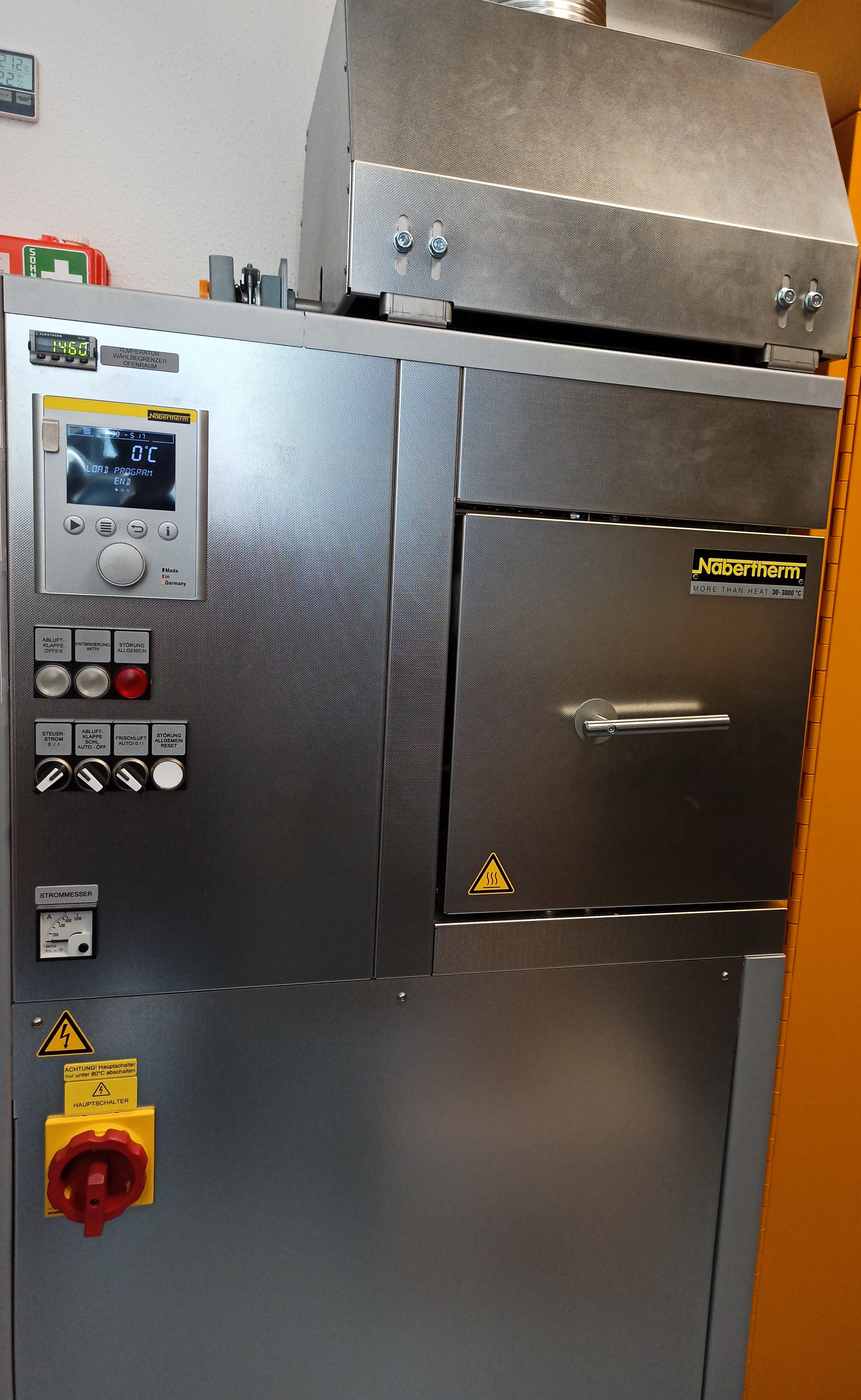 |
Sintering furnace Nabertherm HT16/17 DB50Nabertherm HT 16/17 DB50 furnace is a high-temperature furnace that can be used for various purposes such as: sintering/pre-sintering of ceramic bodies, solid-state materials synthesis, fabrication of different glass phases, etc. Moreover, its debinding feature makes it suitable for heat treatment of 3D printed ceramic green bodies. The main features of Nabertherm HT 16/17 DB50 furnace are:
|
Scanning Mobility Particle Sizer (SMPS)TSI mit DMA 3085 Das Scanning Mobility Particle Sizer Spektrometer ist ein Nanopartikelgrößenmessgerät, das die Anzahlgrößenverteilung luftgetragener Partikel im Submikrometer-Bereich mit Genauigkeit und Präzision bestimmen kann. Es kombiniert die Größenbestimmung über elektrische Mobilität mit der Zählung einzelner Partikel und gibt die Konzentrationen der Nanopartikel in diskreten Größenkanälen aus. Das SMPS kann Partikeldurchmesser bis zu 64 Kanälen pro Dekade auflösen und hat somit gesamt bis zu 109 Kanäle. |
 |