Bacher Research Group
Nanotechnology and nanostructured components are seen as the innovation drivers of the 21st century. Ultra-thin layers or tiny crystals are characterized by unusual properties and open up new applications in electrical engineering and information technology. In this fascinating field of research, the design of nanoscale materials and devices, as well as their microscopic understanding, is a central concern. Microelectronics and optoelectronics are increasingly dominated by nanostructures, but also research areas such as energy science or quantum information technology are often based on nanoscale materials.
In this environment, the research activities at the Chair of Materials in Electrical Engineering can be divided into the following areas:
Graphene and 2D-Materials for Optoelectronics
Graphene as an allotropic form of carbon with a thickness of only one atomic layer is assigned a key function in modern nano and materials technology. Graphene conducts electrical current many times better than the best metallic conductor currently available; it absorbs only 2.7% of the irradiated light and its breaking strength is over 30 times higher than that of Kevlar. In addition to graphene, numerous other 2-dimensional (2D) materials have now been synthesized, including insulators such as hexagonal boron nitride (hBN) or semiconductors such as molybdenum disulphide (MoS2) or tungsten disulphide (WS2). Attractive features of 2D materials include their low thickness of less than one nanometer, their high strength combined with flexibility and the possibility of stacking different classes of materials on top of each other in heterostructures to create new types of functional components. However, a major challenge for the transfer to industrial applications is the scalability of production, processing and device design.
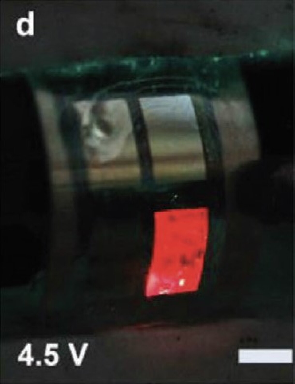
Our field of research includes the production of graphene on various substrates with diameters of up to 4 inches and its integration into novel device architectures. Applications as transparent electrodes in light emitters and as channel material in photoconductors or phototransistors are the focus of our interest. The research work is complemented by investigations into large-area transition metal dichalcogenides. In contrast to graphene, these have a finite band gap and therefore have application potential as an active material in optoelectronics. In various cooperative projects with academic and industrial partners, we are optimizing the manufacturing processes, embedding the 2D semiconductors in device architectures and using them, for example, as ultra-thin and flexible light emitters and photodetectors.

Nanoscale Materials for Energy
If the size of solids is reduced to dimensions in the nanometer range, the material properties change fundamentally: surfaces and interfaces are crucial for functionality and electronic properties must in some cases be described quantum mechanically. This influences energy conversion in light-emitting diodes, solar cells, thermoelectric generators and catalysts, among other things. In order to develop an understanding of the underlying microscopic processes and thus ultimately tailor the materials for defined applications, a detailed analysis of the materials on a nanometer scale is required.
Our diverse analytical methods - electron microscopy, nano-optics and scanning probe microscopy - are able to record current flow and potential distribution as well as optical and structural properties on a nanometer scale and thus correlate material properties and device performance. In collaboration with a wide range of project partners from Germany and abroad, we use this diversity in nanoanalytics to decipher the functionality of metal oxide catalysts, elucidate the local optical properties of micro-LEDs or correlate electrical and thermal conductivity in nanoscale thermoelectric devices.

Nanomaterials for Quantum Technologies
Nanoscale materials open up access to novel quantum technologies in which the quantum mechanical properties of electrons or photons are utilized for information processing, information transmission or information storage. For example, individual colloidal nanocrystals can be used as quantum emitters or magnetic and electrical properties can be coupled through the targeted introduction of transition metals into a nanoscale solid-state matrix. The latter makes it possible, among other things, to use the quantum mechanical property 'spin' of charge carriers to represent information. These future technologies require on the one hand a defined production of customized nanomaterials with suitable doping and on the other hand the development of experimental techniques to study their optical and magnetic properties on a nanometer scale.
We are dedicated to the goal of combining electronic, optical and magnetic functionality in novel nanomaterials and exploring their application potential for quantum technologies. On the one hand, magnetically doped semiconductor nanostructures (quantum dots, nanoclusters, magnetic 2D materials) are investigated with the intention of influencing charge carrier spins via the magnetic dopant atoms and - vice versa - controlling magnetism through optical or electrical stimulation. On the other hand, we are investigating individual nanocrystals to understand their emission properties with a view to applications as quantum emitters. The work is carried out in cooperation with numerous international partners.