Equipment
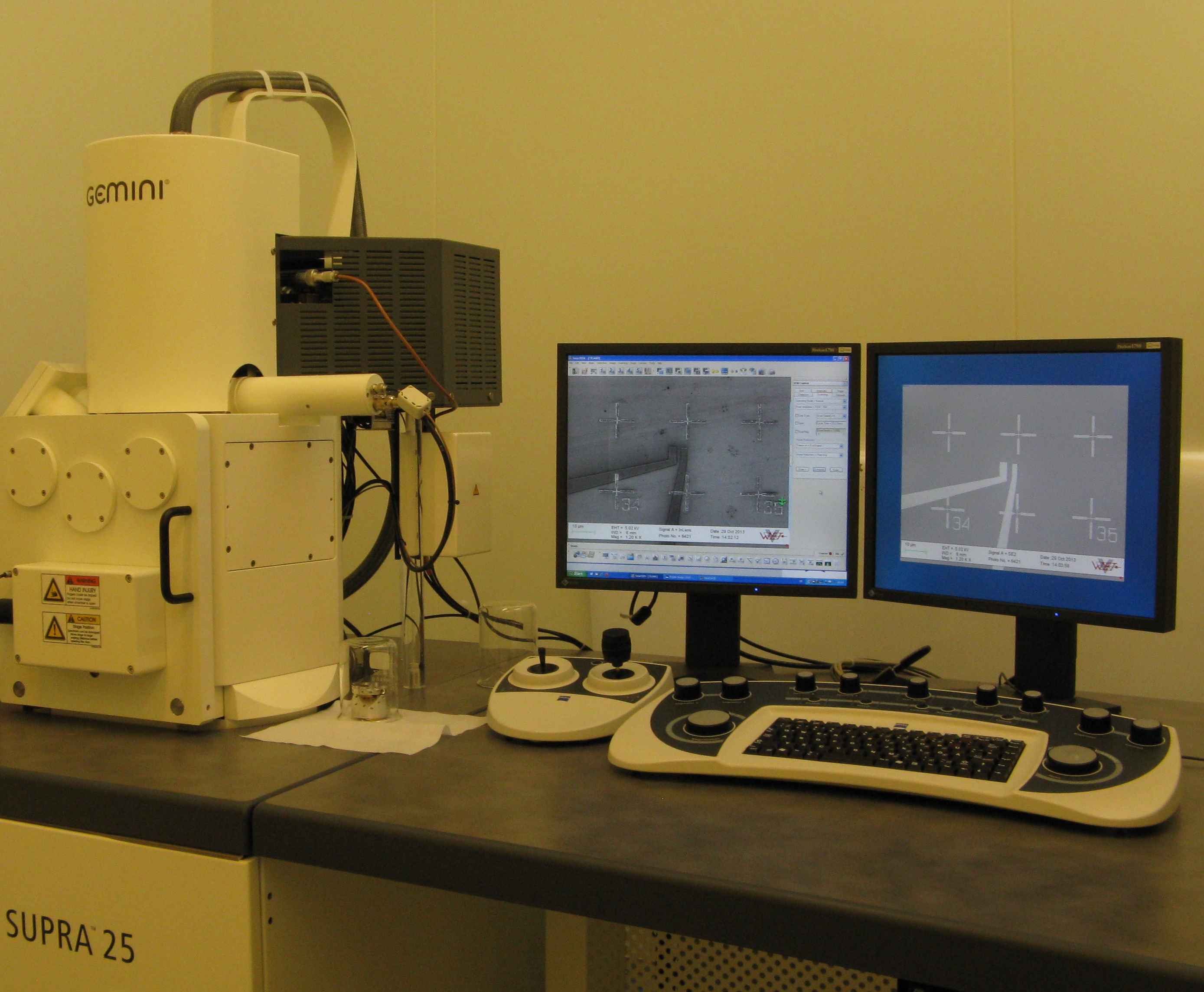
Scanning Electron Microscopy
Our electron microscopy lab includes scanning electron microscopes with acceleration voltages between 0.05 kV and 30 kV and a spatial resolution down to 1.2 nm.
Scanning Force Microscopy
Two Scanning Force Microscopes providing a spatial resolution of <15 nm are currently used for the following techniques:
- Topography analysis (Contact mode, non contact mode, tapping mode)
- Kelvin Probe Force Microscopy
- Local Measurements of electrical Potentials, voltage and current (resolution: few µA, 5 mV)
- Magnetic Force Microscopy

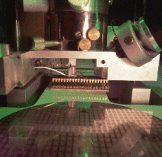
Nanotechnology and Preparation
The institute’s cleanroom provides a 120 m² lab of the classes 100 and 1000. The cleanroom is equipped with:
- Electron beam lithography
- Thermal and electron beam evaporating system, Sputter system
- Mask aligner, Spin Coater
- Ultra sonic bonder, vacuum oven, rapid thermal annealing oven, tube furnace, ozone cleaner
- Equipment for nanoparticle dispersion (tip sonicator, centrifuge
- Microprober
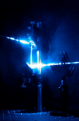
Optical Spectroscopy
Six laser labs are available for different techniques of optical spectroscopy. The focus is on experiments with high spatial and temporal resolution in the temperature range between 2K and 300 K. As options, we can apply static or transient external fields (magnetic field, electric field). Key techniques are as follows:
- Time- and spatially resolved photoluminescence spectroscopy (~ ps, < µm)
- Transient absorption spectroscopy
- g(2) correlation (photon statisctics)
- Magneto optics (micro magnetoluminescence, MCD)
- Micro photoluminescence and micro electroluminescence spectroscopy
- Photocurrent and photo voltage measurements with high spatial resolution (< µm)
- UV-VIS-spectrophotometer, photo diodes for measuring external quantum efficiencies