

Research AG Schmid
Resource-efficient energy conversion
Our research is driven by the goal of enabling resource-efficient energy conversion and developing functional materials and devices with tailored optical and electronic properties. We focus on chalcogenide materials, combining materials research, device concepts, optical design and multiphysics simulation across different length scales.
Our research is built on three closely connected pillars: materials and devices, optical concepts and light and carrier management, and multiphysics simulations. Together, these approaches allow us to investigate materials and structures from their fundamental properties to functional devices and applications.
Chalcogenide materials
Chalcogenides offer a particularly versatile materials platform. Their composition can be varied over a wide range, providing access to materials with tailored structural, optical and electronic properties.
Chalcopyrites solar cells
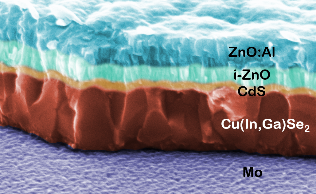
A major focus is on chalcopyrite absorbers for thin-film solar cells. Chalcopyrites combine high absorption coefficients and good stability with the possibility of tailoring their band gap through changes in elemental composition. This is possible within the broad material family (Cu,Ag)(In,Ga,Al)(S,Se)₂. The compositional flexibility makes chalcopyrites particularly interesting for advanced photovoltaic concepts requiring specifically adapted absorber properties.
We have a particular interest in wide-band-gap chalcopyrites, with a focus on Al-containing compounds. Within the DFG project Alchesol, we investigate the properties and potential of these materials for wide-band-gap solar cells. Wide-band-gap absorbers are relevant for concepts such as semitransparent and bifacial solar cells, where the device architecture has to be adapted to make efficient use of light entering from different directions. This includes the investigation of transparent back contacts and optimized front-side structures for efficient carrier collection.
Binary chalcogenides and 2D materials
Our materials research also extends to binary chalcogenides for nanofilms and two-dimensional materials. Their diverse structural and electronic properties make them an attractive platform for emerging nanoscale applications. We investigate their controlled growth as thin films using the ILGAR (ion layer gas reaction) method, with particular interest in the formation and characterization of nanoscale and layered chalcogenide materials. This work includes the DFG project INGA the SNAIL. Together, these activities explore how composition, structure and dimensionality can be used to tailor chalcogenide materials for different functionalities and applications.
Optical concepts and light and carrier management
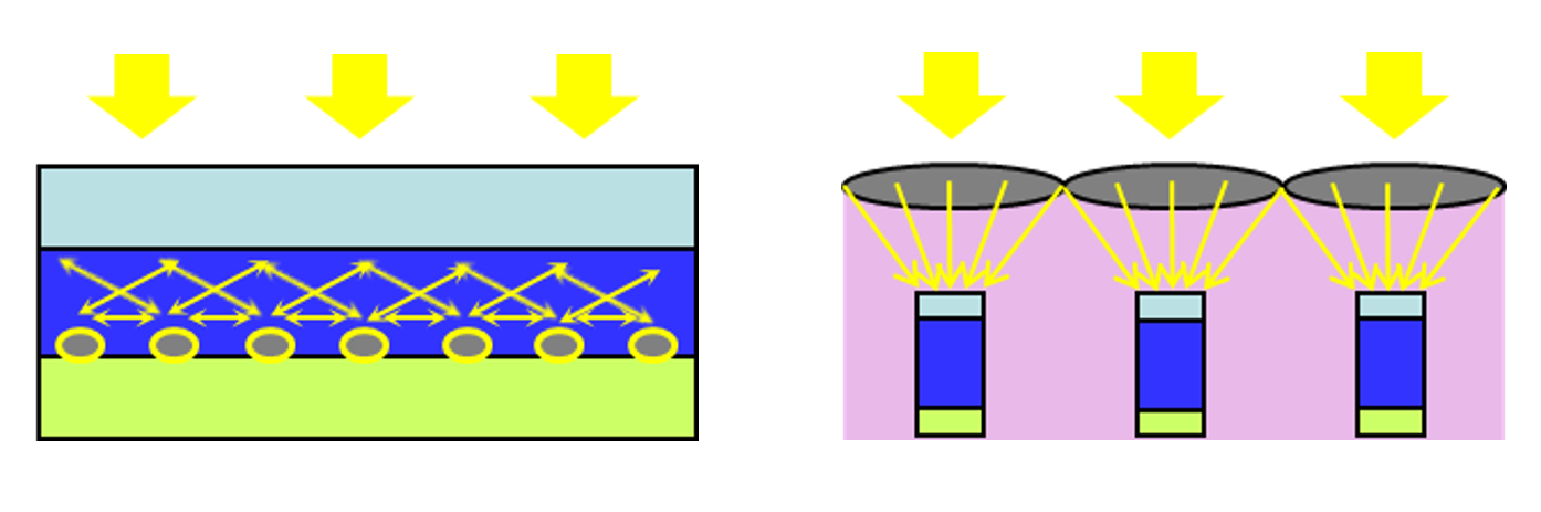
A second pillar of our research is the controlled interaction of light with materials and structures. At the nanoscale, the interaction of electromagnetic fields with structured surfaces and thin films gives rise to nano-optical effects that can be exploited to control how light is coupled, propagated and absorbed. We investigate nanostructures and optical thin-film concepts for light management, with the aim of directing and concentrating light where it can be used most effectively. In photovoltaic devices, this optical design is closely linked to carrier management: the location and distribution of light absorption determine where carriers are generated, while the device structure influences their transport and collection. We therefore consider optical and carrier processes together when designing and evaluating structured devices.
For solar-energy conversion, this includes nanostructured concepts for enhanced light utilization as well as micro-concentrator architectures for concentrating solar radiation. While different in scale and physical implementation, both approaches use tailored structures to control the distribution of light and improve its utilization. The underlying concepts are not restricted to photovoltaics. Tailoring the interaction between light, materials and structures is also relevant to other applications where specific optical functionalities are required.
Multiphysics simulations
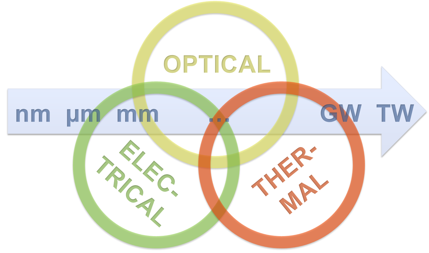
Simulation forms the third pillar of our research and provides a means to connect material properties with device behavior. Since processes in thin films and structured devices are often physically coupled, we develop models that describe their interaction across different physical domains.
For photovoltaic devices, the optical properties of materials and structures determine the spatial distribution of absorbed light and carrier generation. This forms the basis for semiconductor simulations of carrier transport, recombination and collection, which in turn determine the electrical behavior of the device. The resulting energy distribution can additionally be used to investigate thermal effects and heat dissipation. In this way, simulations allow us to follow the influence of material and structural modifications from light absorption through carrier transport to the overall device behavior.
Our work ranges from thin-film calculations, including the tools developed within [RefDex], to two- and three-dimensional numerical simulations based on the finite-element method. These approaches are used to investigate complex geometries, nanostructured devices and micro-concentrator architectures and to identify the physical mechanisms determining their performance.
Connecting materials, light and devices
Our research combines materials development, optical concepts and multiphysics modeling. This enables us to move from the properties of individual materials to structured films and complete devices, while maintaining a close connection between experiment and simulation.
From wide-band-gap Al-containing chalcopyrites for advanced solar cells to binary chalcogenides for nanofilms and 2D materials, we investigate how composition, structure and dimensionality can be exploited to create new functionalities and contribute to more efficient and resource-conscious technologies