About Us
Terahertz Research
Field of High-Frequency Electronics Components
At the Center for Semiconductor Technology and Optoelectronics at UDE, the field of High-Frequency Electronics Components (BHE) focuses on electronic and optoelectronic devices and integrated circuits that utilize the frequency range up to one terahertz. Electromagnetic waves at the highest frequencies between 100 and 1000 GHz are still rarely utilized because suitable components are not yet available. High-frequency components for this spectral range, based on special semiconductor materials and structures, are being researched and developed in this field.
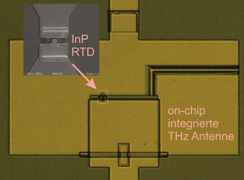
THz Indium Phosphide Resonant Tunneling Diode with Integrated Antenna
The velocity of electrons in a semiconductor is material-dependent and is particularly high in the alloys of the indium phosphide material system. Special device concepts are made possible through heterostructures, including resonant tunneling diodes that operate as oscillators at THz frequencies by utilizing the quantum mechanical tunneling effect, as well as heterojunction bipolar transistors that still provide high gain at the highest frequencies. In the subsequent process technology, the smallest structures are defined and contacts are formed, while simultaneously minimizing parasitic resistances and capacitances in order to achieve the highest frequencies.
The BHE field conducts this research within the framework of the DFG Collaborative Research Center "MARIE" and the EU joint project TeraApps. For optoelectronic devices, the rate of radiative electron-hole recombination, in addition to the motion of the electrons, is crucial for the cutoff frequency. The semiconductor gallium nitride (GaN) has become ubiquitous—white LEDs made from it are found in (almost) every light source today. GaN light sources could also be used for data transmission, for example, in airplanes or trains, to alleviate WiFi congestion. By laterally orienting the GaN crystal, the recombination rate can be significantly increased. This is being investigated in GaN core-shell nanowire structures.
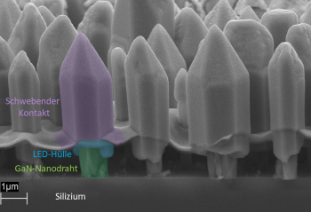
Scanning Electron Microscope Image of the Contacted
GaN Core-Shell Nanowire Structures
for Optical Data Transmission
Special Materials and Growth Processes for Highest Frequencies
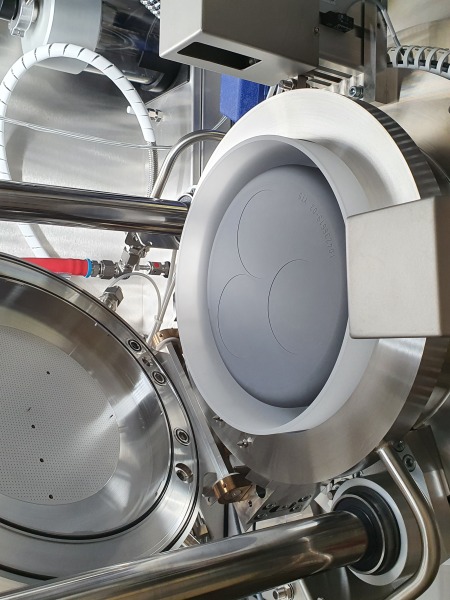
Reactor for Metal-Organic Vapor Phase Epitaxy
for the Production of Semiconductor Layers (MOVPE)
Compound semiconductor layers such as InP are synthetically "grown." Stacks of various compositions—so-called heterostructures—are deposited in epitaxy machines with atomic layer thickness precision. As part of the investment project ForLab SmartBeam funded by the BMBF, a new epitaxy system for InP structures is being established in the BHE field. Atomically thin layers are characterized and optimized using an X-ray diffraction (XRD) system newly acquired through the NRW/EFRE project THzIZ. Another materials research topic in the field involves epitaxial nanowires. In specialized epitaxy processes, self-limiting crystalline wires with a diameter of around 100 nm are created. These are grown in the material systems GaN and Gallium Arsenide (GaAs) in the BHE field and investigated for device applications.
X-ray diffractometer
Exact Designs with High-Performance Computers
As usual, the design is the starting point. Both materials and THz devices, high-frequency circuits, optoelectronic integration, and antenna radiation can be calculated using today’s high-performance computing clusters and specialized software packages. At the ZHO, parallel computers equipped with so-called GPU cards are available, allowing for the simulation of complex structures in a short computation time. Accurate predictions become increasingly important as the manufacturing technology becomes more complex and as integration is pushed to the limit—up to system-level modules.
Nanotechnologies for the Fastest Devices
The shorter the distance that electrons need to travel in the device, the faster the transistors can switch, and the more data can be transmitted using optoelectronic devices. Smaller sizes also lead to reduced capacitances, resulting in shorter charging times for the structures. Both of these goals are achieved through a nanoscale process technology. Special methods for structure definition using electron beams and nanoimprint techniques, as well as plasma-assisted etching, are employed in the cleanroom of the ZHO to realize terahertz devices. A significant portion of the building is dedicated to filtering and conditioning the laboratory air to ensure that nanoscale structures can be produced without defects.
Vertical integration techniques enable the monolithic integration of antenna structures with active THz transmitters and receivers. A new focus is currently emerging beyond the semiconductor process in the EFRE-funded "THz Integration Center"—due to the short wavelength of less than 1 mm in the THz range, the housing must be included in the design of the THz components. THz modules compatible with the semiconductor chips are manufactured using precision tools and 3D printing processes.
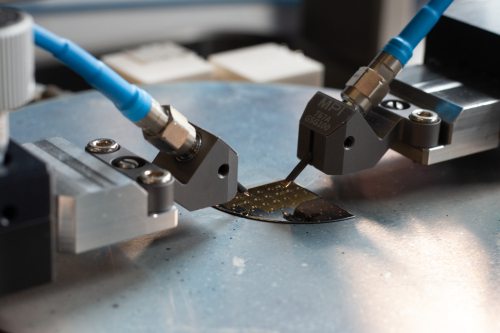
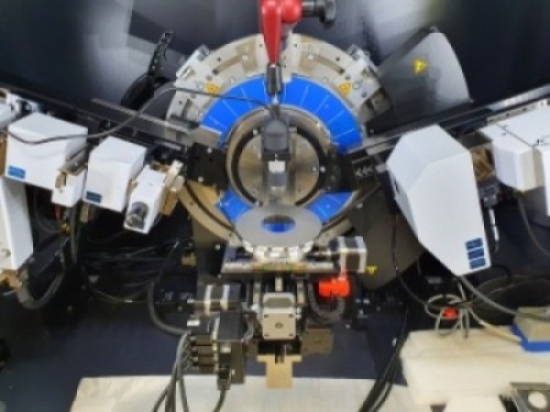
On-Wafer Measurements for Characterization of THz Devices and
Circuits Manufactured in the Cleanroom