Time-of-Flight secondary ion mass spectrometry (TOF-SIMS)
What can a time-of-flight secondary ion mass spectrometer do?
The abbreviation TOF-SIMS is an acronym for the combination of secondary ion mass spectrometry (SIMS) with a time-of-flight (TOF) mass analyser.
The sample to be analysed is bombarded with a primary ion beam with a kinetic energy of a few keV. The ions collide with the surface, releasing their energy and generating a shock cascade. This leads to the detachment of individual surface atoms and molecules, or of clusters and fragments. Some of these secondary particles are present as ions and can be analysed separately according to their mass.
The time-of-flight principle is used for mass separation. Particles of different mass reach different velocities at the same acceleration voltage. The accelerated particles travel a certain distance in the analyser and reach the detector at different times, the lighter the particle the faster it is. Since times can be measured with very high accuracy, this method achieves a very high spectral mass resolution and gives a very accurate picture of the sample surface and its composition. The procedure is shown in the film in Figure 1.
With this method one achieves a spatial resolution < 100 nm, with a surface sensitivity to the first 1-2 layers of the sample. Depth profiles with a depth accuracy of < 1nm and a measurement speed of up to 10µm/h are achievable.
With the Integrated Focused Ion Beam Source (FIB) it is possible to cleanly generate cross-sectional areas of highly porous surfaces and layered structures with strongly varying ion etch rates and then to investigate these cross-sections. The creation of such a crater is shown in the film in Figure 2. The crater has a size of about 30µmx15µm with a depth of about 20µm. Duration about 6h.
At ICAN we use the TOF.SIMS 5 from Ion-TOF.
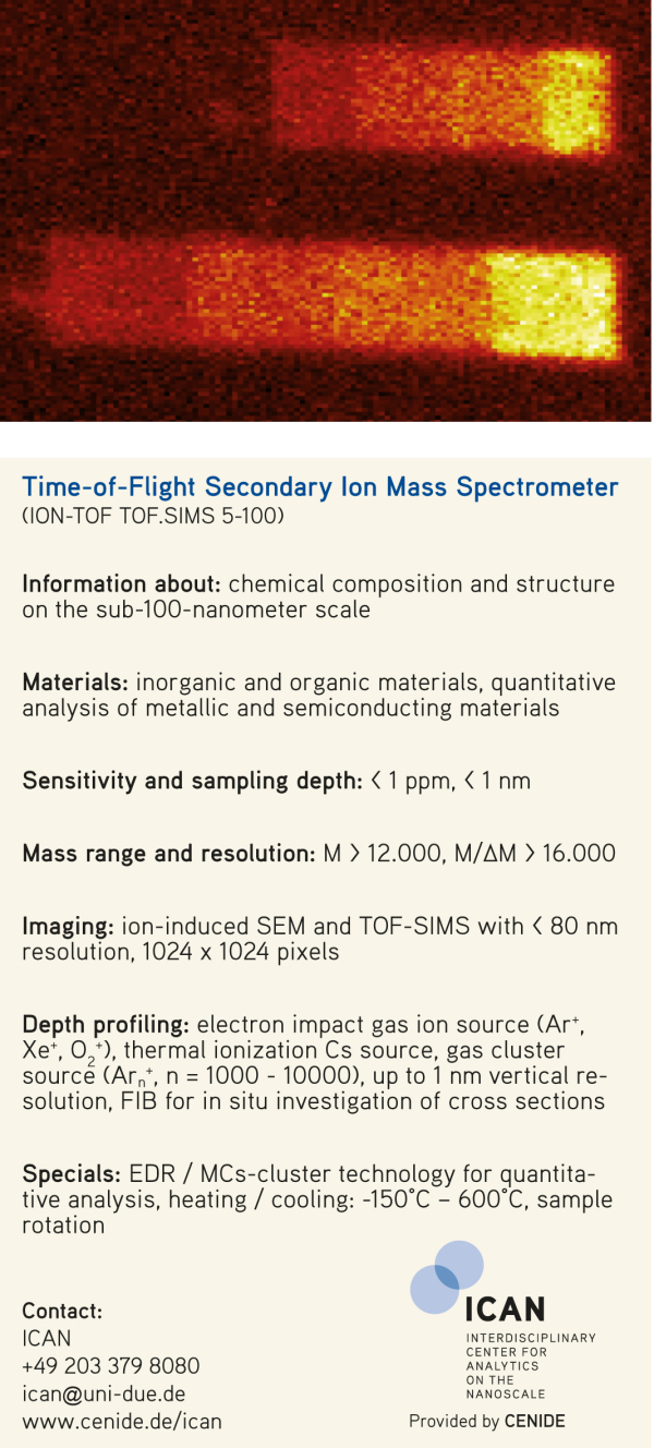
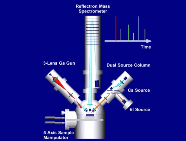
Figure 1: Illustration of the Time-of-Flight principle. Animation provided by the Ion-TOF GmbH.
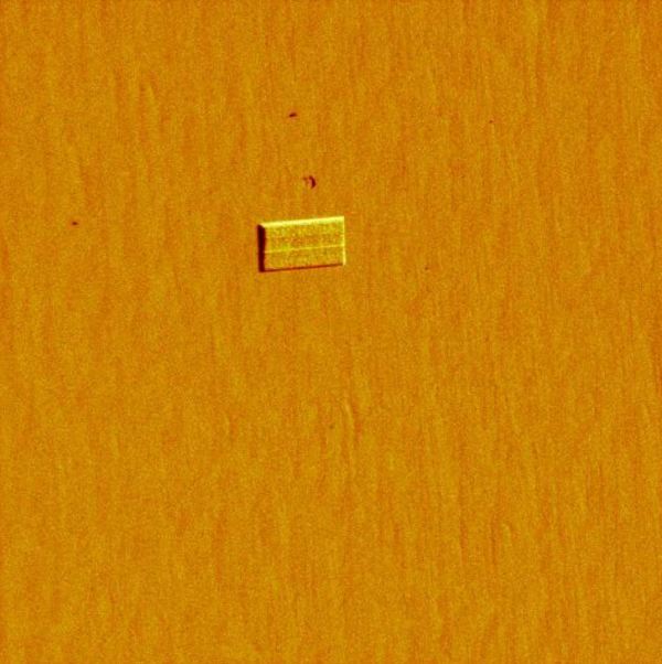
Figure 2: Secondary electron images of the creation of an FIB crater in doped diamond to examine the exposed cross-sectional area. Size of the crater about 30µm x 15µm x 20µm. Duration about 6h.
Depth profiling
Figure 3 shows the mass spectrum of a europium-doped aluminium oxide layer on silicon on a linear and logarithmic scale. Since this technique measures differences in the time of flight, the conversion of this time scale into a mass scale is very important. As a result, the evaluation of the data often takes considerably more time than its generation.
The logarithmic plot shows the enormous sensitivity of the technique. It is possible to measure doping concentrations down to the ppm range.
Figure 4 shows the intensity curve of the aluminium and europium signal as a function of the sputtering time. Between the recording of 2 mass spectra, the surface was bombarded with fast oxygen molecules to expose deeper atomic layers. In this way, a depth profile of the material is generated. In this example, it can be seen that the europium concentration increases towards the depth, has a maximum at the interface to the silicon and then decreases again towards the silicon.
There are several reasons why the transition from Al2O3 to silicon is not arbitrarily sharp. In this case, the high roughness of the Al2O3 surface was largely responsible for this. The aluminium oxide layer examined was about 8 µm thick.
TOF-Sims is not a technique to directly determine total concentration with one measurement. The reason for this is that the removal rates and ionisation probability of a given element/molecule strongly depends on the matrix in which it is located.
For example, a certain amount of doping of boron in silicon would give a significantly different signal intensity than the same amount of boron in diamond. Therefore, ideally one needs a reference sample for each measurement, with the same matrix, where the concentration of the dopant is known.
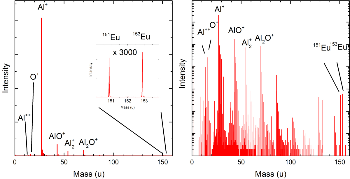
Figure 3: Mass spectrum of europium-doped alumina on linear and logarithmic scales.
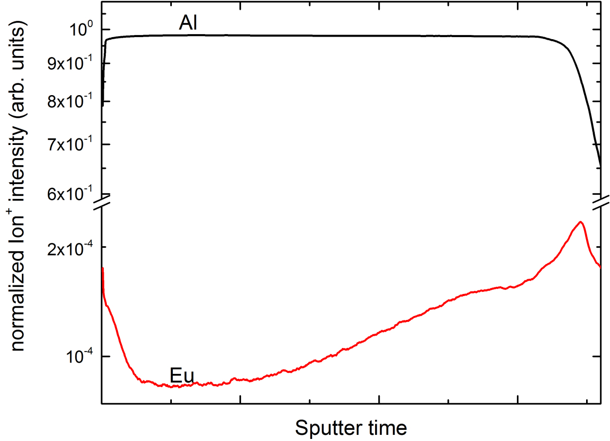
Figure 4: Course of the intensity of the Al+ and Eu+ signals as a function of the ion etching time (etched with oxygen). The thickness of the Al2O3 layer was approx. 8 µm.
Ihr Ansprechpartner für das TOF-SIMS:
ICAN - Interdisciplinary Center for Analytics on the Nanoscale
47057 Duisburg
Functions
-
Wissenschaftliche/r Mitarbeiter/in, Center for Nanointegration Duisburg-Essen
-
apl. Professor/in, Physikalische Chemie

Current lectures
No current lectures.
Past lectures (max. 10)
-
WiSe 2025
-
WiSe 2024
-
WiSe 2023
-
WiSe 2022
-
WiSe 2021
The following publications are listed in the online university bibliography of the University of Duisburg-Essen. Further information may also be found on the person's personal web pages.
-
Laser-Induced Iron Doping of Spinel Thin Film Electrocatalyst : Impact of Pulsed Laser Processing on Surface Cobalt Oxide Doping and Oxygen Evolution Reaction ActivityIn: ChemCatChem, Vol. 18, 2026, Nr. 2, e01233DOI (Open Access)
-
Diffusion of Eu, Ce and Lu in orthopyroxeneIn: Geochimica et Cosmochimica Acta, Vol. 410, 2025, pp. 85 – 100DOI (Open Access)
-
Interaction of 2-propanol with predominantly SrO- and TiO2-terminated SrTiO3(100) surfaces studied by vibrational sum frequency spectroscopyIn: Catalysis Science and Technology, Vol. 13, 2023, Nr. 17, pp. 4988 – 4995DOI (Open Access)
-
N-Doped porous carbons obtained from chitosan and spent coffee as electrocatalysts with tuneable oxygen reduction reaction selectivity for H₂O₂ generationIn: RSC Advances, Vol. 13, 2023, Nr. 33, pp. 22777 – 22788DOI (Open Access)
-
Beneficial Effects of Low Iron Contents on Cobalt‐Containing Spinel Catalysts in the Gas Phase 2‐Propanol OxidationIn: ChemCatChem, Vol. 14, 2022, Nr. 18, e202200472DOI (Open Access)
-
Auf Spurensuche im Nanokosmos : Katalyseforschung im Interdisciplinary Center for Analytics on the NanoscaleIn: Unikate: Berichte aus Forschung und Lehre, 2021, Nr. 57: Katalyse : Alles andere als oberflächlich, pp. 139 – 148DOI, Online Full Text (Open Access)
-
Segregation-Enhanced Epitaxy of Borophene on Ir(111) by Thermal Decomposition of BorazineIn: ACS Nano, Vol. 15, 2021, Nr. 4, pp. 7421 – 7429
-
The Effect of Water on the 2-Propanol Oxidation Activity of Co-Substituted LaFe₁−CoₓO₃ PerovskitesIn: Chemistry - A European Journal, Vol. 27, 2021, Nr. 68: Special Issue: Contemporary Challenges in Catalysis, pp. 17127 – 17144DOI (Open Access)
-
Experimental evidence for the separation of thermally excited bipolar charge carries within a p-n junction : A new approach to thermoelectric materials and generatorsIn: Journal of Applied Physics, Vol. 125, 2019, Nr. 18, 184502
-
Lead diffusion in CaTiO₃ : A combined study using Rutherford backscattering and TOF-SIMS for depth profiling to reveal the role of lattice strain in diffusion processesIn: American Mineralogist, Vol. 104, 2019, Nr. 4, pp. 557 – 568
-
UV-light assisted patterned metallization of textile fabricsIn: Applied Surface Science, Vol. 436, 2018, pp. 1093 – 1103
-
Adjusting the catalytic properties of cobalt ferrite nanoparticles by pulsed laser fragmentation in water with defined energy doseIn: Scientific Reports, Vol. 7, 2017, Nr. 1, pp. 13161DOI, Online Full Text (Open Access)
-
Gradual modification of ITO particle's crystal structure and optical properties by pulsed UV laser irradiation in a free liquid jetIn: Dalton Transactions, Vol. 46, 2017, Nr. 18, pp. 6039 – 6048
-
Laser-Induced Functionalization of Organo/Carbon Interfaces for Selective Adsorption of Au Nanoparticles in Microsized DomainsIn: Langmuir, Vol. 33, 2017, Nr. 35, pp. 8686 – 8692
-
Laser-induced surface activation of biocomposites for electroless metallizationIn: Surface and Coatings Technology, Vol. 311, 2017, pp. 104 – 112
-
Resonant laser processing of nanoparticulate Au/TiO2 films on glass supports : Photothermal modification of a photocatalytic nanomaterialIn: Surface Science, Vol. 650, 2016, pp. 57 – 63
-
Surface-enhanced Raman spectroscopy on laser-engineered ruthenium dye-functionalized nanoporous goldIn: Applied Surface Science, Vol. 374, 2016, pp. 19 – 22
-
Photothermally induced bromination of carbon/polymer bipolar plate materials for fuel cell applicationsIn: Applied Surface Science, Vol. 336, 2015, pp. 85 – 88
-
Poly(N,N-dimethylaminoethyl methacrylate) Brushes : pH-Dependent Switching Kinetics of a Surface-Grafted Thermoresponsive PolyelectrolyteIn: Langmuir, Vol. 31, 2015, Nr. 49, pp. 13426 – 13432
-
Resonant photothermal laser processing of hybrid gold/titania nanoparticle filmsIn: Applied Surface Science, Vol. 336, 2015, pp. 48 – 52
-
Chemical functionalization of carbon/polymer bipolar plate materials via oxygen plasma activation and subsequent silanizationIn: Surface and Coatings Technology, Vol. 240, 2014, pp. 255 – 260
-
Photothermal Laser Fabrication of Micro- and Nanostructured Chemical Templates for Directed Protein ImmobilizationIn: Langmuir, Vol. 30, 2014, Nr. 49, pp. 14841 – 14848
-
Photothermal laser microsintering of nanoporous goldIn: Langmuir, Vol. 30, 2014, Nr. 24, pp. 7190 – 7197
-
Fabrication of chemical templates via selective laser-induced desorption of hexadecanethiol self-assembled monolayersIn: Applied Surface Science, Vol. 278, Laser materials processing for micro and nano applications, E-MRS 2012 Symposium V, 2013, pp. 57 – 61
-
Fabrication of periodic surface topographies via sequential photothermal laser microsintering of silicon nanoparticle filmsIn: Applied Surface Science, Vol. 278, 2013, pp. 278 – 283
-
Femtosecond-laser processing of nitrobiphenylthiol self-assembled monolayersIn: Applied Surface Science, Vol. 278: Laser materials processing for micro and nano applications, E-MRS 2012 Symposium V, 2013, pp. 43 – 46
-
Hofmeister Effect of Sodium Halides on the Switching Energetics of Thermoresponsive Polymer BrushesIn: Macromolecular Rapid Communications, Vol. 34, 2013, Nr. 5, pp. 417 – 422
-
Laser-doping of crystalline silicon substrates using doped silicon nanoparticlesIn: Thin Solid Films, Vol. 548, 2013, pp. 437 – 442
-
Sintering of thin titanium dioxide nanoparticle films via photothermal processing with ultraviolet continuous-wave lasersIn: Applied Surface Science, Vol. 278, Laser materials processing for micro and nano applications, E-MRS 2012 Symposium V, 2013, pp. 336 – 340
-
VerNETZungen : Integrierte Nanopartikel-Synthese und -Verarbeitung im NanoEnergieTechnikZentrumIn: Unikate: Berichte aus Forschung und Lehre, 2013, Nr. 43: NanoEnergie – Materialentwicklung für eine nachhaltige Energieversorgung, pp. 26 – 41DOI, Online Full Text (Open Access)
-
Photothermal laser processing of thin silicon nanoparticle films : On the impact of oxide formation on film morphologyIn: Applied Physics A: Materials Science and Processing, Vol. 106, 2012, Nr. 4, pp. 853 – 861
-
Substrate-mediated effects in photothermal patterning of alkanethiol self-assembled monolayers with microfocused continuous-wave lasersIn: Beilstein Journal of Nanotechnology, Vol. 3, 2012, Nr. 1, pp. 65 – 74DOI (Open Access)
-
Probing the intrinsic switching kinetics of ultrathin thermoresponsive polymer brushesIn: Angewandte Chemie International Edition, Vol. 50, 2011, Nr. 19, pp. 4513 – 4516
-
Micro- and nanopatterning of functional organic monolayers on oxide-free silicon by laser-induced photothermal desorptionIn: Small, Vol. 6, 2010, Nr. 17, pp. 1918 – 1926
-
Nonlinear femtosecond laser processing of alkylsiloxane monolayers on surface-oxidized silicon substratesIn: Journal of Vacuum Science and Technology A: Vacuum, Surfaces, and Films, Vol. 28, 2010, Nr. 4, pp. 814 – 817
-
Photothermal micro- and nanopatterning of organic/silicon interfacesIn: Langmuir, Vol. 26, 2010, Nr. 9, pp. 6826 – 6831
-
Photothermally induced bromination and decomposition of alkylsiloxane monolayers on surface-oxidized silicon substratesIn: Journal of Vacuum Science and Technology A: Vacuum, Surfaces, and Films, Vol. 28, 2010, Nr. 4, pp. 834 – 837
-
Self-assembled organic monolayers as high-resolution resists in rapid nonlinear processing with single femtosecond laser pulsesIn: Applied Physics A: Materials Science and Processing, Vol. 101, 2010, Nr. 3, pp. 461 – 466
-
Sub-wavelength patterning of organic monolayers via nonlinear processing with continuous-wave lasersIn: New Journal of Physics (NJP), Vol. 12, 2010, pp. 125017DOI, Online Full Text (Open Access)
-
Temporal stability of photothermally fabricated micropatterns in supported phospholipid multilayersIn: Journal of Vacuum Science and Technology A: Vacuum, Surfaces, and Films, Vol. 28, 2010, Nr. 4, pp. 953 – 957
-
Direct Laser Patterning of Soft Matter: Photothermal Processing of Supported Phospholipid Multilayers with Nanoscale PrecisionIn: Small, Vol. 5, 2009, Nr. 18, pp. 2099 – 2104
-
Laser-induced local dehydroxylation on surface-oxidized silicon substrates: mechanistic aspects and prospects in nanofabricationIn: Applied Physics A: Materials Science and Processing, Vol. 94, 2009, Nr. 1, pp. 95 – 103
-
Photothermally induced microchemical functionalization of organic monolayersIn: ChemPhysChem, Vol. 10, 2009, Nr. 12, pp. 2000 – 2003
-
Surface-initiated polymerization on laser-patterned templates : morphological scaling of nanoconfined polymer brushesIn: Langmuir, Vol. 25, 2009, Nr. 20, pp. 12393 – 12398
-
Subwavelength patterning of alkylsiloxane monolayers via nonlinear processing with single femtosecond laser pulsesIn: Applied Physics Letters (APL), Vol. 92, 2008, pp. 223111
-
Oriented growth of osteoblast-like cells on two-dimensionally structured films of functionalized calcium phosphate nanoparticles on a silicon substrateIn: Advanced Engineering Materials, Vol. 9, 2007, pp. 1077 – 1081
-
Self-assembled organic templates for the selective adsorption of gold nanoparticles into confined domains
24th European Conference on Surface Science (ECOSS-24) ; 4-8 September 2006, Paris, France,In: Surface Science, Vol. 601, 2007, Nr. 18, pp. 3916 – 3920 -
1D Nanofabrication with a Micrometer-Sized Laser SpotIn: Nano Letters, Vol. 6, 2006, Nr. 10, pp. 2358 – 2361
-
Direct laser patterning of octadecylsiloxane monolayers on surface-oxidized silicon substrates : Indications for a photothermal excitation mechanismIn: Surface Science, Vol. 600, 2006, Nr. 18, pp. 4034 – 4038
-
Laser-assisted decomposition of alkylsiloxane monolayers at ambient conditions : rapid patterning below the diffraction limitIn: Applied Physics A: Materials Science and Processing, Vol. 82, 2006, Nr. 4, pp. 689 – 695
-
Laser-assisted fabrication of submicron-structured hydrophilic/ hydrophobic templates for the directed self-assembly of alkylsiloxane monolayers into confined domainsIn: Applied Physics A: Materials Science and Processing, Vol. 82, 2006, Nr. 1, pp. 15 – 18
-
Preparation of two-dimensionally patterned layers of functionalised calcium phosphatenanoparticles by laser direct writingIn: Journal of Materials Chemistry, Vol. 16, 2006, Nr. 19, pp. 1798 – 1802
-
Characterization of the telomere complex, TERF1 and TERF2 genes in muntjac species with fusion karyotypesIn: Experimental Cell Research, Vol. 306, 2005, Nr. 1, pp. 64 – 74
-
Preparation of stacked organosiloxane bilayers on hydrophilic and hydrophobic silicon substrates by spin coatingIn: Thin Solid Films, Vol. 488, 2005, Nr. 1-2, pp. 124 – 131
-
Characterization of ancestral chromosome fusion points in the Indian muntjac deerIn: Chromosoma, Vol. 112, 2004, Nr. 5, pp. 213 – 220
-
Imaging surface topographical changes during plastic deformation of a metal with chemical wave patternsIn: Surface Science, Vol. 548, 2004, Nr. 1-3, pp. 163 – 169
-
Preparation of Submicron-Structured Alkylsiloxane Monolayers Using Prepatterned Silicon Substrates by Laser Direct WritingIn: Langmuir, Vol. 20, 2004, Nr. 9, pp. 3525 – 3527
-
An AFM study of the growth kinetics of the self-assembled octadecylsiloxane monolayer on oxidized silicon
7th International Conference on Nanometer-Scale Science and Technology and the 21st European Conference on Surface Science (NANO-7 / ECOSS-21) ; 24-28 June 2002, Malmö, Sweden,In: Surface Science, Vol. 532-535, 2003, pp. 963 – 969 -
Mutations in the polyglutamine binding protein 1 gene cause X-linked mental retardationIn: Nature Genetics, Vol. 35, 2003, Nr. 4, pp. 313 – 315DOI (Open Access)
-
Two-dimensional aggregation of species with weak and strong bonding interactions : Modeling the growth of self-assembled Alkylsiloxane monolayersIn: Langmuir, Vol. 19, 2003, Nr. 17, pp. 6590 – 6593
-
Reaction of sulfur dioxide with Ag(110)–p(2x1)-O : a LEED, TPRS, and STM investigationIn: Surface Science, Vol. 504, 2002, pp. 223 – 234
-
Pattern formation in restricted geometries : The NO+CO reaction on Pt(100)In: The Journal of Chemical Physics (JCP), Vol. 112, 2000, Nr. 15, pp. 6795 – 6803DOI (Open Access)
-
Nonlinear processing and multiphoton ablation of self-assembled monolayers for application as ultrathin resists and in biochemical sensorsIn: Optically Induced Nanostructures: Biomedical and Technical Applications / König, Karsten; Ostendorf, Andreas (Eds.). Berlin [u.a.]: de Gruyter, 2015, pp. 117 – 139
-
Laser Patterning of Silanized Carbon/Polymer Bipolar Plates with Tailored Wettability for Fuel Cell ApplicationsIn: Laser Surface Modification and Adhesion / Mittal, K. L.; Bahners, Thomas (Eds.). Hoboken, New Jersey: John Wiley and Sons, Inc, 2014, pp. 263 – 287
-
Micro-patterning of self-assembled organic monolayers by using tunable ultrafast laser pulsesIn: Frontiers in ultrafast optics: biomedical, scientific, and industrial applications XIV / SPIE photonics west , 2 - 5 February 2014, San Francisco, California, United States. Bellingham, Wash.: SPIE, 2014
-
Sub-wavelength patterning of self-assembled organic monolayers via non-collinear optical parametric amplifierIn: ICALEO 2013 - 32nd International Congress on Applications of Lasers and Electro-Optics / 32nd International Congress on Applications of Lasers and Electro-Optics, ICALEO 2013, Miami, FL, United States, 6 October 2013 through 10 October 2013, 2013, pp. 893 – 897
-
Fabrication, laser structuring and field emission properties of carbon nanowallsIn: 25th International Vacuum Nanoelectronics Conference (IVNC 2012) / International Vacuum Nanoelectronics Conference, Jeju, South Korea, 9 - 13 July 2012. Piscataway, NJ: IEEE, 2012, pp. 354 – 355
-
Electron emission of laser-structured carbon nanowalls on Si and stainless steel substratesIn: 24th International Vacuum Nanoelectronics Conference (IVNC), 2011 / International Vacuum Nanoelectronics Conference, 18 - 22 July 2011, Historische Stadthalle Wuppertal, Germany / Klümper, Andreas (Eds.). Piscataway: IEEE, 2011, pp. 139 – 140
-
Preparation of organic monolayers on uniform and patterned silicon substratesIn: Physical chemistry of interfaces and nanomaterials II: 6 - 8 August 2003, San Diego, California, USA II / Optical Science and Technology, SPIE's 48th Annual Meeting, 2003, 06.-08.08.2003, San Diego, California, United States / Lian, Tianquan; Dai, Hai-Lung (Eds.). Bellingham [u.a.]: SPIE, 2003, pp. 9 – 23
-
Photothermal laser processing of thin silicon nanoparticle films : prospects in photovoltaic applications
1st International Conference on Materials for Energy, 4. - 8. Juli 2010 Karlsruhe, Germany,Karlsruhe, 2010