Thin Films
AlSb films
Polycrystalline AlSb-films, based on AlSb-heterocycles of the type [R2AlSb(SiMe3) 2]2 (R = Et, i-Bu) were deposited on Al2O3 substrates in a cold-wall-reactor in the temperature range between 375 and 550 °C.[1]

Figure 1: AlSb-films of [Et2AlSb(SiMe3)2]2 and [i-Bu2AlSb(SiMe3)2]2
The carbon content of the obtained AlSb-films is below the detection limit of WDX (wavelength dispersive X-ray analysis). However, there is a temperature-dependent incorporation of Si in the films, based on the decomposition of the SiMe3-ligands. The Si-content increases strongly with rising substrate temperature. The optimum temperature window for the deposition of crystalline AlSb (XRD) from these specific precursors is between 400 °C and 450 °C.
GaSb films
Crystalline GaSb-films were deposited in a cold wall reactor on Si (100)-substrates from completely alkyl-substituted heterocycles of the type [R2GaSbR' 2]x in the temperature range between 350 and 550 °C. Our present investigations concentrate on [t-Bu2GaSbEt2]2, which is easily obtained by reaction of t-Bu3Ga with Sb2Et4.[2]
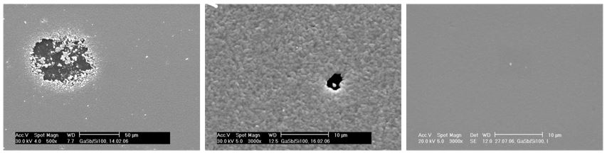
Figure 2: SEM images of various GaSb films (Tsubstr.(Si(100)) = 425 °C); SEM-image of a GaSb-film illustrating the Vollmer-Weber growth
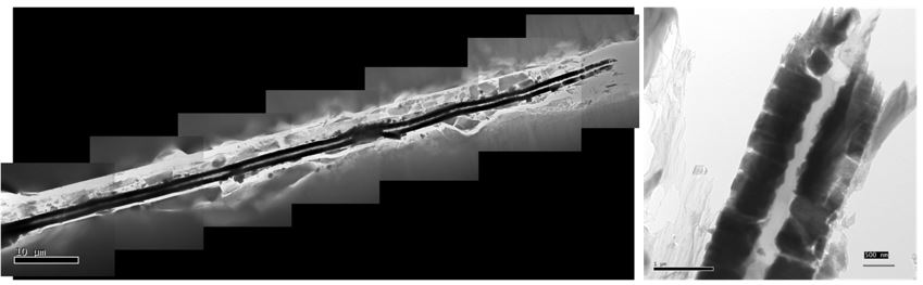
Figure 3: TEM images (thin section) of a GaSb film (black) deposited at 450 °C on a Si (100) substrate (light) deposited The polycrystalline structure of the films is evident.
The resulting polycrystalline material films show a homogeneous surface morphology. The film thickness depends substantially on the substrate temperature (kinetically controlled growth area) and the film growth follows a Vollmer-Weber mechanism.
XRD Experiments show that only at temperatures above 375 °C crystalline GaSb films (sphalerite type) are deposited, while at lower substrate temperatures only amorphous materials are obtained.
The chemical composition of the resulting films was determined by EDX (Ga:Sb = 1.00 - 1.01). EELS- and AES-studies (C, O), sputter-experiments showed that the contaminations of the films with C and O is only at the surface. AFM images demonstrate a very homogeneous film growth with surface roughness in the range of 10-25 nm.
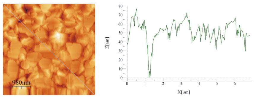
Figure 4: AFM photographs of a deposited GaSb-film at 450 °C on Si (100).
References
[1] H. S. Park, S. Schulz, H. Wessel, H. W. Roesky, Chem. Vap. Deposition, 1999, 5, 179.
[2] a) S. Schulz, S. Fahrenholz, A. Kuczkowski, W. Assenmacher, A. Seemayer, A. Hommes, K. Wandelt Chem. Mater. 2005, 17, 1982; b) S. Fahrenholz, A. Kuczkowski, S. Schulz, K. Wandelt, A. Seemayer, W. Assenmacher, Electrochem. Soc. Proc. 2005, 9, 730, c) S. Schulz, D. Schuchmann, S. Fahrenholz, A. Kuczkowski, W. Assenmacher, F. Reilmann, N. Bahlawane, K. Kohse-Höinghaus, Surf. Coat. Technol. 2007, 201, 9071.
Go back: Gas phase-based Synthesis
For more: Nanowires