Nanowires
GaSb nanowires
The simple pyrolysis of GaSb-adducts of type R3GaSbR'3 in sealed glass ampoules in the temperature range 350-500 °C yields GaSb crystallites.[1] Their carbon content is below the detection limit of the electron energy loss spectroscopy (EELS), while oxygen is present as a surface contamination.
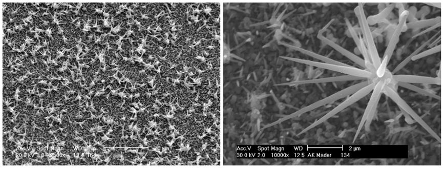
Figure 1: REM picture of GaSb dendrites as-obtained from thermolysis reactions of (t-Bu)3Ga–Sb(t-Bu)3 in a closed glass ampule at 450 °C.
Dendritic-like growth was observed at high decomposition temperatures while isolated GaSb nanowires were rather obtained at lower temperatures (250 - 350 °C) as well as from other adducts such as [t-Bu3Ga]2[Sb2Et4]. The nanowires were characterized in detail by EDX, EELS (Sb-mapping) and high-resolution transmission-electron-microscopy (HR-TEM).[2]
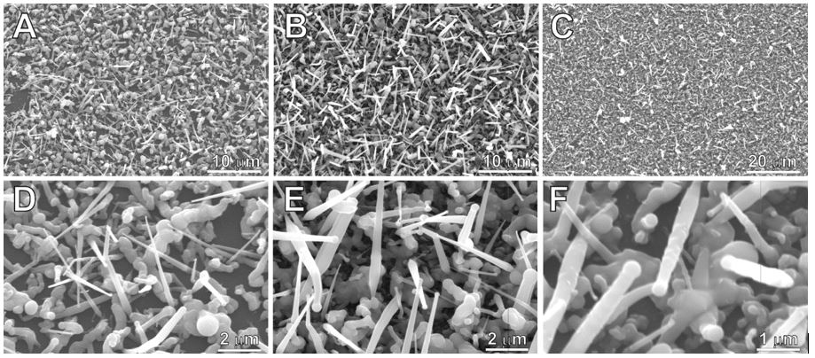
Figure 2: SEM images showing GaSb dendrites as-obtained from (t-Bu)3Ga–Sb(i-Pr)3 at Tdec. = 275 °C (A, D), 300 °C (B, E), and 325 °C (C, F).
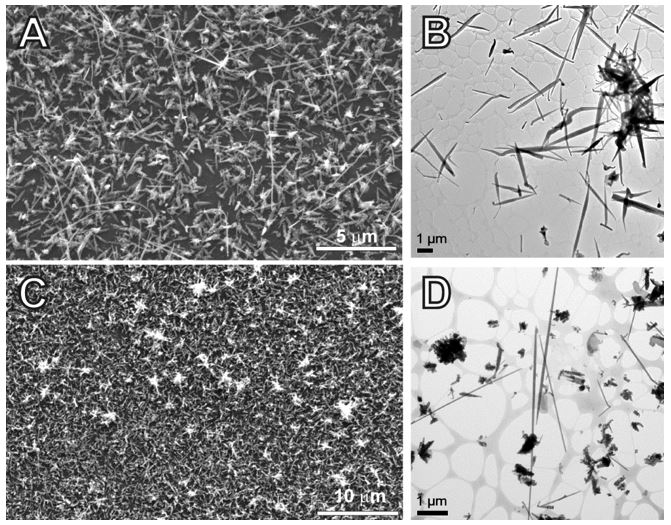
Figure 3. SEM and TEM images of GaSb nanowires obtained from [t-Bu3Ga]2[Sb2Et4] at Tdec. = 250 °C (top) and 400 °C (bottom). D shows the formation of GaSb nanowires with high aspect ratio.

Figure 4. SAED pattern with simulation as an overlay and HRTEM image of of GaSb nanowires obtained from [t-Bu3Ga]2[Sb2Et4] at Tdec. = 250 °C in <110> zone axis. The indicated distances of 353 and 305 pm correspond to {111} and {200} lattice fringes, respectively.
In addition, a rather controlled self-catalyzed growth of GaSb nanowires using 90 nm-sized Ga droplets, which were pre-deposited on Si(100) substrates by thermal decomposition of t-Bu3Ga, was achieved with Sb2Et4 at 250 °C.[2] Ga droplets have been shown in the past to initiate nanowire growth of a variety of materials such as Si and Ge.[3] The pyrolysis experiments clearly showed that Ga droplets act as an initiator (catalyst) for the GaSb nanowire growth and the growth of the nanowires, which occured according to the so-called VLS mechanism (vapor-liquid-solid),[4] showed a strong dependency on the pyrolysis temperature.
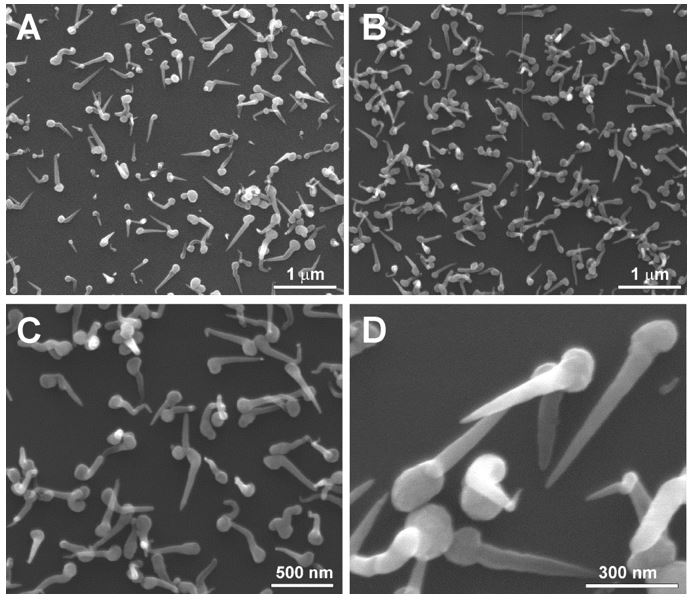
Figure 5. SEM images showing tapered GaSb nanowires formed at Tsubstrate = 250 °C with different deposition times (tdep.(Sb2Et4) = 90 min A, C; 120 min B, D).
The decomposition of t-Bu3Ga forms a Ga-droplet on the substrate, which catalyse the decomposition of the Sb-precursor, resulting in an enrichment of the Ga-droplet with elemental Sb. After exceeding the saturated solution level, the crystallization starts at the liquid-solid interface and the nanowire is formed and the Ga-droplet is preserved on the top of the whisker.

Figure 6. Formation of nanowires by the VLS mechanism
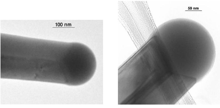
Figure 7. Nanowires of crystalline GaSb, at the top is the (amorphous) Ga-droplet visible.
Bismuth nanowires
Bismuth is a semimetal, promising very large quantum size effects due to the small effective mass of charge carriers and very low carrier density.[5] Bi-nanowires, were predicted to undergo a transition from semimetal to semiconductor with diameters smaller than 50 nm (77 K), or <10 nm (25 °C). In addition, Bi-nanowires are discussed as interesting thermoelectric materials and different procedures for the production of nanowires and nanocrystals have been developed.[6] However, typical procedures such as hydrothermal methods,[7] particularly electrochemical deposition in porous aluminium oxide templates and others,[8,9] typically bares problems related to the low melting point of Bi (271.3 °C).
In the course of our studies we focused our investigations on the deposition of Bi-nanowires by MOCVD process. Bi nanowires were obtained with trialkylbismuthanes as well as dibismuthanes under very mild reaction conditions, below 200 °C using Bi2Et4.
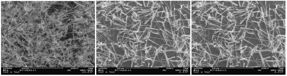
Figure 8. SEM images of Bi-nanowires
References
[1] A. Kuczkowski, S. Schulz, W. Assenmacher, J. Mater. Chem. 2001, 11, 3241.
[2] S. Schulz, M. Schwartz, A. Kuczkowski, W. Assenmacher, J. Cryst. Growth 2010, 312, 1475.
[3] H. Chandrasekaran, G. U. Sumanasekara, M. K. Sunkara, J. Phys. Chem. B 2006, 110, 18351.
[4] R. S. Wagner, W. C. Ellis, Appl. Phys. Lett. 1964, 4, 89.
[5] a) S. B. Cronin, Y.-M. Lin, O. Rabin, M. R. Black, J. Y. Ying, M. S Dresselhaus, P. L. Gai, J.-P. Minet, J.-P. Issi, Nanotechnol. 2002, 13, 653. b) N. Garcia, Y. H. Kao, M. Strongin, Phys. Rev. B 1972, 5, 2029.
[6] a) J. Heremans, C. M. Thrush, Phys. Rev. B 1999, 59, 12579; b) Y. M. Lin, X. Z. Sun, M. S. Dresselhaus, Phys. Rev. B 2000, 62, 4610; c) Y.-M. Lin, O. Rabin, S. B. Cronin, J. Y. Ying, M. S Dresselhaus, Appl. Phys. Lett. 2002, 81, 2403.
[7] a) R. L. Fu, S. Xu, Y. N. Lu, J. J. Zhu, Cryst. Growth Des. 2005, 5, 1379; b) W. Z. Wang, B. Poudel, Y. Ma, Z. F. Ren, J. Phys. Chem. B 2006, 110, 25702.
[8] a) L. Li, Y. Zhang, G. Li, L. Zhang, Chem. Phys. Lett. 2003, 378, 244; b) J. Heremans, C. M. Thrush, Y. M. Lin, S. Cronin, Z. Zhang, M. S. Dresselhaus, J. F. Mansfield, Phys. Rev. B 2000, 61, 2921; c) J. Heremans, C. M. Thrush, Z. Zhang, X. Sun, M. S. Dresselhaus, J. Y. Ying, D. T. Morelli, Phys. Rev. B 1998, 58, R10091.
[9] a) Y. Gao, H. Niu, C. Zeng, Q. Chen, Chem. Phys. Lett. 2003, 367, 141; b) Y. Xu, Z. Ren,W. Ren, G. Cao, K. Deng, Y. Zhong, Nanotechnol. 2008, 19, 115602; c) P. Chiu, I. Shih, Nanotechnol. 2004, 15, 1489; d) G. Bhimarasetti, M. K. Sunkara, J. Phys. Chem. B 2005, 109, 16219.