Gas phase-based Synthesis
Semiconducting III/V-Materials
Due to their physical properties semiconductors group III/V materials are of considerable interest for technical applications. Binary, ternary and quaternary III/V materials find various applications in opto- and microelectronics or photovoltaics. InP, GaAs or GaN, which is unique in the manufacture of LEDs and lasers for the blue or green spectral range, are of particular interest. The physical properties within this material group vary considerably.
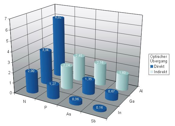
Figure 1: Band gabs of binary III/V materials ME at 300 K [eV]
The classical method for the synthesis of these materials is the Liquid-Phase Epitaxy (LPE). However, alternative techniques such as Molecular Beam Epitaxy (MBE) and especially the Metal Organic Chemical Vapor Deposition (MOCVD) have become more important. The MOCVD-process belongs to one of the most important commercial process since this low-cost process allows the deposition of thin films on large substrates. As a consequence, the MOCVD-process was used for the deposition of binary and multinary thin films of the light homologues of group 15 elements, N, P and As (e.g. GaN, InP, GaAs). In contrast, the CVD-deposition of the corresponding binary antimonides, which show the lowest band gaps (1.60 (AlSb), 0.67 (GaSb) and 0.16 eV (InSb)) and highest electron mobility within the III/V materials and therefore find interesting technical applications in long wave length optoelectronic components, infrared detectors and in photovoltaic applications, faces several fundamental problems:[1]
a) Vapor pressure of elemental antimony
The low vapor pressure of elemental antimony requires the strict control of a certain R3Sb/MR3-concentration ratio during pyrolysis to prevent the deposition of elemental antimony on the substrate.[2]
b) Kinetic-controlled growth process
At the required low deposition temperatures (T <550 °C) AlMe3 and GaMe3 are only incompletely decomposed. This leads on the one hand to a kinetic-controlled film growth and, on the other hand, promotes the incorporation of carbon contaminations into the growing material films due to incomplete decomposition of the precursors.[3]
c) Instability of SbH3 and the lack of alternative Sb-precursors
Formally the most suitable precursors such as SbH3, MeSbH2 or Me2SbH can`t be used for this process due to their thermal instability.[4] In contrast, trialkylstibines (SbMe3, SbEt3) are thermally very stable and require high substrate temperatures. This is problematic due to the low melting points of the group 13-antimonides (e.g. InSb 525 °C). The most promising Sb-precursors are currently i-Pr3Sb, i-Pr2SbH and Sb(NMe2)3. However, its low vapor pressure causes problems.[5]
Goals
Besides the development of new (classical) precursors for Sb- and Bi-containing materials we pursue an alternative approach. Instead of using two precursors we concentrate on compounds which contain the desired combination of elements already preformed at the molecular level. These compounds, known as single-source-precursors, include R3MER'3 adducts and [R2MER'2]x heterocycles.[6] They are less sensitive toward oxidation and hydrolysis and typically show lower decomposition temperatures. Compounds of this type were also identified as reaction intermediates in classical dual source-CVD processes.[7] Since the beginning of our work almost no MSb-precursors were known. Only Cowley et al. reported on the deposition of GaSb and InSb films from single-source-precursors.[8] We now have a large pool of potentially suitable precursors, in particular Lewis acid-base-adducts R3MSbR'3 and heterocycles [R2MSbR'2]x ,that have been investigated in specially designed hot-wall or cold-wall-reactors with simple pyrolysis studies and MOCVD-processes. With some of the precursors crystalline AlSb- and GaSb-films have been deposited.
References
[1] a) A. Aardvark, N. J. Mason, P. J. Walker, Prog. Crystal Growth and Charact. 1997, 35, 207; b) R. M. Biefeld, Mater. Sci. Eng. R. 2002, 36, 105.
[2] a) J. Shin, A. Verma, G. B. Stringfellow, R.W. Gedridge Jr., J. Crystal Growth 1995, 151, 1; b) A. Subekti, E.M. Goldys, M. J. Paterson, K. Drozdowicz-Tomsia, T. L. Tansley, J. Mater. Res. 1999, 14, 1238; c) A. Subekti, E. M. Goldys, T. L. Tansley, J. Phys. Chem. Sol. 2000, 61, 537.
[3] a) C. A. Wang, S. Salim, K. F. Jensen, A. C. Jones, J. Crystal Growth 1997, 170, 55; b) J. S. Ford, F. P. Howard, G. J. Davies, J. Crystal Growth 1998, 188, 159.
[4] a) M. A. Todd, G. Bandari, T. H. Baum, Chem. Mater. 1999, 11, 547; b) B. C. Harrison, E. H. Tompkins, Inorg. Chem. 1962, 1, 951; c) O. Sugiura, H. Kameda, K. Shiina, M. Matsumura, J. Electron. Mater. 1988, 17, 11.
[5] J. Shin, A. Verma, G. B. Stringfellow, R. W. Gedridge, J. Crystal Growth 1994, 143, 15.
[6] a) A. H. Cowley, R. A. Jones, Angew. Chem. 1989, 101, 1235; b) A. C. Jones, Chem. Soc. Rev. 1997, 101; c) S. Schulz, Coord. Chem. Rev. 2001, 215, 1.
[7] a) E. G. J. Staring, G. J. B. M. Meekes, J. Am. Chem. Soc. 1989, 111, 7648; b) F. C. Sauls, L. V. Interrante, Z.P. Jiang, Inorg. Chem. 1990, 29, 2989.
[8] A. H. Cowley, R. A. Jones, C. M. Nunn, D. L. Westmoreland, Chem. Mater. 1990, 2, 221.
Go back: Material Synthesis
For more: Thin Films