ALD deposition
4.2.2.2 ALD deposition
Sb2Te3 thin films were grown via atomic layer deposition (ALD) in a closed-build chamber type reactor.[1] Silicon wafers with a top-layer of 300 nm thermal silicon oxide were used as substrate. During the whole process, the precursor materials (Et3Si)2Te on the tellurium (Te) side and SbCl3 on the antimony (Sb) side were kept at constant source temperatures of 77 °C and 55 °C, respectively. Alternate pulsing of the precursor gases into the reaction chamber leads to the formation of solid and stable Sb2Te3 films with subsequent elimination of Et3SiCl (dehalosilylation reaction) during the self-limited surface reaction.[2] No film deposition could be observed below a reaction chamber temperature of 80 °C. Since the growth rate of the films strongly decreases with increasing reaction chamber temperature,[3] the deposition temperature was set to 80 °C resulting in a maximal growth rate of 0.16 Å/cycle. SEM of Sb2Te3 films, deposited with different numbers of cycles, showed a Volmer-Weber island growth mechanism. The deposited Sb2Te3 forms discontinuous islands, getting larger with increasing number of pulses. Above 600 pulse-cycles (d ~ 10 nm) a continuous and electrically conductive Sb2Te3- film was formed. The island growth mechanism imprints its structure to the surface texture and determines the roughness of the films, which leads to nanocrystalline Sb2Te3.
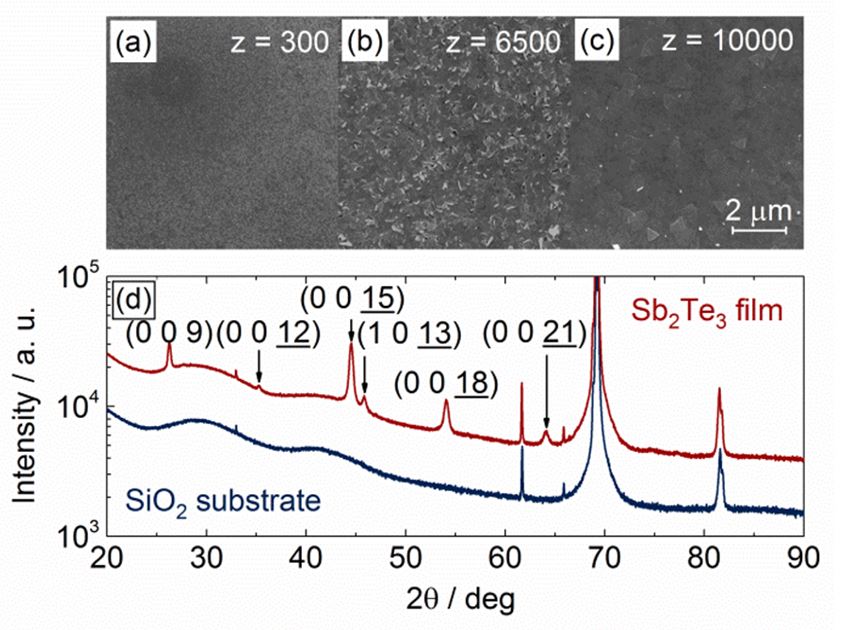
Figure 1: Scanning Electron Micrographs of the surface of ALD grown Sb2Te3 thin films, with 300 (a), 6500 (b) and 10000 (c) growth-cycles. X-ray diffraction pattern of the SiO2 substrate reference (dark blue) and a 32 nm thick Sb2Te3 film (red) (d). The peaks correspond to literature values.
In addition to Sb2Te3 thin films, we also investigated the ALD deposition of Bi2Te3 thin films, which were finally prepared from bis(trimethylsilyl)telluride and bismuth(III) chloride at relatively low temperatures (100 to 160 °C) by atomic layer deposition and the grain sizes were systematically varied in the range of 50 to 200 nm. We found that three different growth modes are possible by controlling the nucleation kinetics and/or employing the epitaxial substrates:
(i) Polycrystalline growth via dense, random nucleation and growth.
(ii) van der Waals epitaxy on SiO2/Si substrates by suppressed nucleation events, resulting in the CVD graphene-like texture.
(iii) Hetero-epitaxy on single crystalline Al2O3 and GaAs substrates.
Top-view SEM micrographs in Figs. 2(a-d) show a clear evolution of the grain growth in the range of ~50 to ~200 nm in average diameter (Davg) by increasing the growth temperature during ALD (Tsub, 100 - 160 °C in this study, including 220 °C results as a control). The grain growth in the resulting Davg is apparent even with increasing 10 °C as proved by AFM [Figs. 2(e-g) and 2(j)]. Although Davg looks uniform when observed in a top view, its distribution became significant in the samples grown at over 140 °C [Fig. 2(h) and the inset of Fig. 2(i)], probably as a result of anisotropic grain growth. Indeed, the development of the ab-planes whose direction is perpendicular to the substrate is evident [Figs. 2(d) and 2(i)]. Such an effect might be apparent in the growth rate as well [Fig. 2(k)]. In general, the ideal ALD growth is believed to have a minimal temperature dependency because the CVD components are avoided and it takes place in the self-limiting regime.
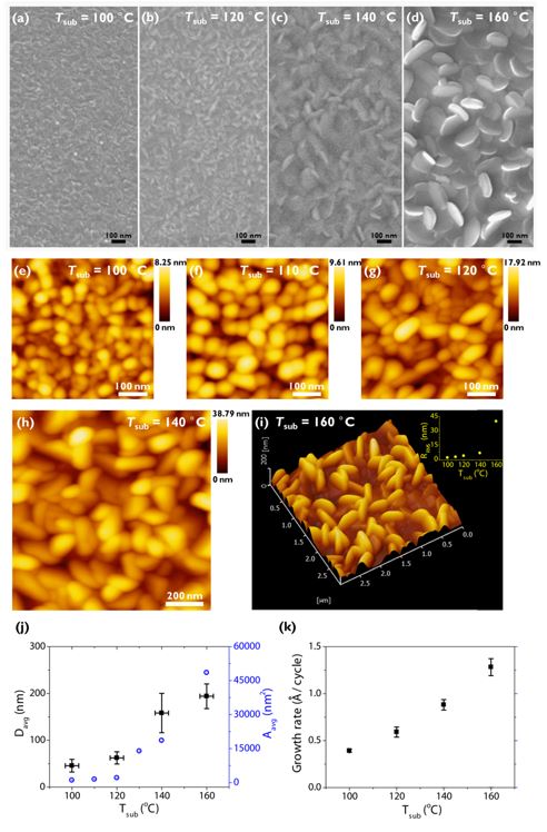
Figure 2: Surface analysis of Bi2Te3 layers grown at different Tsub. Top-view SEM micrographs at (a) Tsub = 100 °C, (b) 120 °C, (c) 140 °C, and (d) 160 °C. AFM height images at (e) Tsub = 100 °C, (f) 110 °C, (g) 120 °C, (h) 140 °C, and (i) 160 °C. The inset of panel (i) shows a plot of root mean square roughness (RRMS) versus Tsub. (j) Plots of the average diameter (Davg)/the average grain area (Aavg) versus Tsub and (k) the growth rate versus Tsub.
The films were investigated by XRD and HR-TEM. Fig. 3(a) shows the XRD results of ALD Bi2Te3 layers grown at different Tsub, showing mostly low-intensity peaks, i.e., (0,0,0,3n) according to the powder diffraction data (JCPDS no. 150863), and indicative of the anisotropic nature of Bi2Te3. The development of a high order peak (at around 57°) out of the 100 % peak (015) implies the formation of a polycrystalline structure rather than a textured structure. This was testified in the morphologies as shown in Figs. 2(d) and 2(i). A HR-TEM image taken at a sample grown at Tsub = 160 °C exhibits the layered Bi2Te3 with grain boundaries [Fig. 3(b)]. XPS results showed the presence of surface oxides although HR-TEM testified no detectable impurity phases within the films (Tsub = 100 - 160 °C).
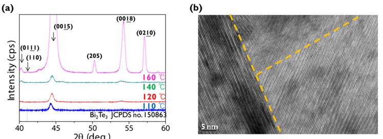
Figure 3: (a) XRD results of Bi2Te3 films grown at different Tsub and (b) TEM image of a sample at Tsub = 120 °C, showing the grain boundaries (dotted yellow line) and the layered structures of Bi2Te3, a quintuple ~ 1 nm.
We monitored the conductivity, Seebeck coefficient and power factor of all samples from 50 to 400 K. By increasing the growth temperature, remarkably, we observed the gradual defect activation from the nominal p-type to n-type in our binary end compound, Bi2Te3 without alloying. The present results give us an insight on the optimization of thermoelectric materials not only by nanostructuring (i.e., phonon engineering) but also by controlled defect activation (i.e., electron engineering).
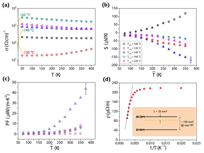
Figure 4: Electrical and thermoelectric characterization of our Bi2Te3 thin films grown at different Tsub. (a) The electrical conductivity σ, (b) the Seebeck coefficient S, (c) the power factor PF, and (d) an Arrhenius plot (Tsub = 120 °C), extracting a impurity level below the bulk conduction band minima (BCBM). All figures share the symbols/colors as in the inset of panel (b).
References
[1] S. Zastrow, J. Gooth, T. Boehnert, S. Heiderich, W. Toellner, S. Heimann, S. Schulz, K. Nielsch, Semicond. Sci. Technol. 2013, 28, 035010.
[2] Knapas, K., Hatanpää, T., Ritala, M., and Leskelä, M. February Chem. Mater. 2010. 22, 1386.
[3] Pore, V., Hatanpää, T., Ritala, M., and Leskelä, M. March J. Am. Chem. Soc. 2009, 131, 3478.
Go Back:4.2.2.1 Chemical Vapor Deposition
For more:4.2.3 Metals