Chemical Vapor Deposition
4.2.2.1 Chemical Vapor Deposition
Metal organic chemical vapour deposition (MOCVD) is a promising technical process for the deüpositipon of high-quality, including epitaxial, thin films and has been shown in the past to produce crystalline binary (Sb2Te3 , Bi2Te3) and multinary group 15/16 material films.[1] Trialkylstibines SbR3 (R = Me, Et) and dialkyltellanes TeR'2 (R = Et, i-Pr, t-Bu) are typically used as molecular precursors,[2] but these often require high pyrolysis temperatures, forcing the incorporation of impurities such as carbon in the material film. Therefore, there is a strong demand for alternative metal organic precursors. Single-source precursors are promising candidates for low-temperature deposition processes.[3]
We demonstrated that (Et2Sb)2Te can be used as MOCVD single source precursor for the synthesis of highly stoichiometric Sb2Te3 films with very low antisite defect concentrations at temperatures as low as 200 °C.[4] Unfortunately, the Sb2Te3 films were rather polycrystalline, consisting of hexagonal Sb2Te3 nanoplates. In the case of the (Et2Sb)2Te precursor, the low substrate temperatures (200 °C) limited the diffusion mobility of the deposited Sb and Te atoms, hence avoiding the formation of a flat film. In contrast, higher substrate temperatures yielded flat Sb2Te3 films, but these were contaminated by elemental antimony.
In contrast, epitaxial Sb2Te3 films were deposited using i-Pr3Sb and Et2Te2 between 350 and 400 °C an Al2O3(0001) substrates.[5] An almost linear increasing growth rate with increasing substrate temperature was found in the temperature range from 350 °C to 400 °C, reaching 750 nm in 15 min at 400 °C. These findings point to a kinetically-controlled growth process. The film obtained at 400 °C consists of large Sb2Te3 flakes, while a film deposited at 350 °C also showed hexagonal Sb2Te3 nanocrystals, which adopt perpendicular orientations to the film surface. The higher substrate temperature results in higher decomposition rates and affects the mobility of the adatoms, which increases with increasing substrate temperature, yielding larger Sb2Te3 nanoflakes. Moreover, the surface morphology (flatness) of the film improved with increasing substrate temperature.
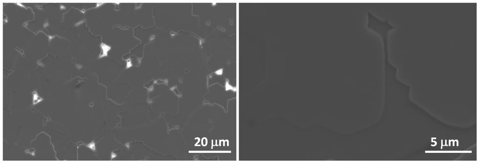
Figure 1: SEM picture of the Sb2Te3 film deposited at 400 °C on Al2O3(0001). Bright spots result from small holes in the film.
The AFM micrograph shows regular terraces of 1 nm height, which correspond to one quintuple layer of the layered tetradymite-type structure of Sb2Te3. These findings indicate a layered growth as was also observed in MBE-grown Sb2Te3 thin films.
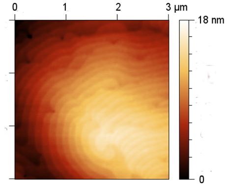
Figure 2: AFM photograph of a Sb2Te3 film deposited at 400 °C on an Al2O3(0001) substrate.
The X-ray diffractogram (XRD) of the Sb2Te3 film deposited at 400 °C clearly proved the formation of highly crystalline Sb2Te3 films. All reflection peaks can be indexed on the basis of the structure of rhombohedral Sb2Te3. In addition, a small reflex of the Al2O3(0001) substrate is visible at 41.6°. The peaks in the diffractogram correspond to (00l) planes, pointing to a c-axis oriented growth as was previously reported for Sb2Te3 films grown by MBE and MOCVD.

Figure 3: 2-θ XRD pattern of the Sb2Te3 film deposited at 400 °C on an Al2O3(0001) substrate; peaks are labelled (JCPDS-ICDD card 15-0874); the asterisk (*) corresponds to the Al2O3(0001) substrate.
The band structure of the surface was also characterized by photoelectron spectroscopy (PES). The overview ARPES spectra of the valence band show intense structures around 0.8 eV binding energy and more faint features near EF which are well discernible at 16 and 17 eV photon energy but not at 21 eV, where their photoemission intensity is weak due to final state effects. This surface state has previously been studied theoretically and in ARPES experiments at selected photon energies (21.2 eV), 55 eV, 8.44 and 24 eV, respectively.[6]
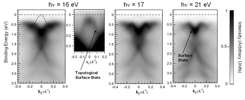
Figure 4: Overview ARPES spectra of the valence band. The topological surface state forming Dirac cone near the Fermi level (0 eV binding energy) is best observed at 16 eV photon energy. Another surface state with massive character appears as higher binding energy and is best seen at 21 eV.
Very recently, we succeeded in the MOCVD deposition of epitaxial ternary (SbxB1-x)2Te3 (0<x<1) thin films at 400 °C using the tailor-made precursors Et2Te2, i-Pr3Sb and Et3Bi, which were characterized by XRD.[7]
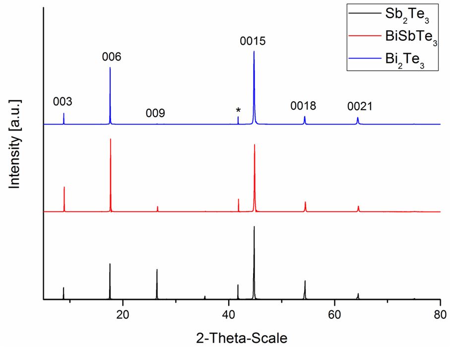
Figure 5: X-ray diffractograms of Sb2Te3 (black), Bi2Te3 (blue) and (Bi0.5Sb0.5)2Te3 films (red) grown on Al2O3(0001) at 400 °C; the marked reflex (*) corresponds to the substrate Al2O3(0001).
Fig. 6 shows the 006 pole figures of (Bi0.5Sb0.5)2Te3 films grown on Al2O3(0001) (left) and Si(100) (right) at 400 °C. The epitaxial (Bi0.5Sb0.5)2Te3 film grown on Al2O3 only shows a single peak, while the 0006 pole figure of the film grown on Si shows a pattern due to the hexagonal discs standing on the substrate surface. The epitaxial relationship of the film and the Al2O3 substrate is (Bi0.5Sb0.5)2Te3 (001)ǁAl2O3(0001).
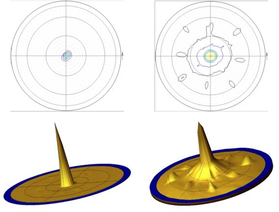
Figure 6: 006 pole figures for (Bi0.5Sb0.5)2Te3 films grown on Al2O3(0001) (left) and Si(100) (right).
The films grown on Al2O3(0001) substrates show a very smooth surface morphology as was shown by SEM, AFM and TEM, while those grown on Si(100) are rather polycrystalline. The chemical composition of the crystalline films (XRD) was investigated by EDX and XPS and the in-plane transport properties of the MOCVD grown (BixSb1−x)2Te3 films were determined by Hall effect measurements using the van der Pauw geometry in order to determine, how the carrier concentration n, the carrier mobility µ and the conductivity σ are affected by the bismuth content. For pure Sb2Te3 films, a high carrier mobility of about 330 cm2V-1s-1 was found, comparable to values measured for bulk single crystals and other high quality Sb2Te3 films grown by ALD, MOCVD and MBE. With increasing bismuth content x, the carrier mobility decreases to a minimum value of 244 cm2V-1s-1 for x = 0.63. With further increasing bismuth content, the mobility increases up to 260 cm2V-1s-1 for pure Bi2Te3.
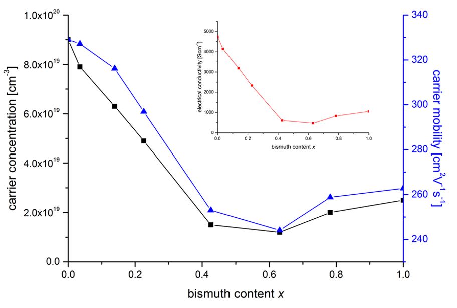
Figure 7: Carrier concentration and mobility of (BixSb1-x)2Te3 films grown at 400 °C on Al2O3(0001).
References
[1] a) T. J.Groshens, Jr. R. W. Gedridge, C. K. Lowe-Ma, Chem. Mater. 1994, 6, 727; b) R. Venkatasubramanian, T. Colpitts, B. O’Quinn, S. Liu, N. El-Masry, M. Lamvik, Appl. Phys. Lett. 1999, 75, 1104; b) A. Giani, A. Boulouz, F. P. Delannoy, A. Foucaran, A. Boyer, B. Aboulfarah, A. Mzerd, J. Mater. Sci. Lett. 1999, 18, 541; c) J. H. Kim, Y. C. Jung, S. H. Suh, J. S. Kim, J. Nanosci. Nanotechnol. 2006, 6, 3325; d) J. S. Lee, S. Brittman, D. Yu, H. Park, J. Am. Chem. Soc. 2008, 130, 6252.
[2] H. B. Singh, N. Sudha, Polyhedron 1996, 15, 745.
[3] J. S. Ritch, T. Chivers, M. Afzaal, P. O’Brien, Chem. Soc. Rev. 2007, 36, 1622.
[4] G. Bendt, S. Schulz, S. Zastrow, K. Nielsch, Chem. Vap. Deposition 2013, 19, 235.
[5] G. Bendt, S. Zastrow, K. Nielsch, P. S. Mandal, J. Sánchez-Barriga, O. Rader, S. Schulz, J. Mater. Chem. A 2014, 2, 8215.
[6] a) H. Zhang, C.-X. Liu, X.-L. Qi, X. Dai, Z. Fang, S.-C. Zhang, Nat. Phys. 2009, 5, 438; b) G. Wang, X. Zhu, J. Wen, X. Chen, K. He, L. Wang, X. Ma, Y. Liu, X. Dai, Z. Fang, J. Jia, Q. Xue, Nano Res. 2010, 3, 874; c) C. Pauly, G. Bihlmayer, M. Liebmann, M. Grob, A. Georgi, D. Subramaniam, M. R. Scholz, J. Sánchez-Barriga, A. Varykhalov, S. Blügel, O. Rader, M. Morgenstern, Phys. Rev. B 2012, 86, 235106, d) L. Plucinski, A. Herdt, S. Fahrendorf, G. Bihlmayer, G. Mussler, S. Döring, J. Kampmeier, F. Matthes, D. E. Bürgler, D. Grützmacher, S. Blügel, C. M. Schneider, J. Appl. Phys. 2013, 113, 053706.
[7] S. Schulz, G. Bendt, J. Sonntag, A. Lorke, U. Hagemann, W. Assenmacher, Semicond. Sci. Technol. 2015, 30, 085021.