Group 15 Chalcogenides
4.3.1.3 Group 15 Chalcogenides
Group 15/16 chalcogenides of the general type M2E3 (M = Sb, Bi; E = S, Se, Te) have a long standing history in material sciences. Sb2S3 is of particular interest for technical applications in sensitized solar cells (SSCs) due to its attractive bandgap energy (∼1.7 eV) and high extinction coefficient (1.8 × 105 cm-1) in the visible region, allowing the fabrication of heterojunction solar cells with over 5% of power conversion efficiency under 1 sun = 1 kWm-2 illumination,[1] while Sb2Se3 is a semiconductor with ~1 eV bandgap,[2] which exhibits a high Seebeck coefficient[3] with a fast amorphous crystalline transition,[4] rendering it very attractive for technical applications in photovoltaic,[5] phase change memory[6] and in thermoelectric (TE) devices.[7] The thermoelectric properties of Sb2Te3 are even better compared to Sb2Se3, rendering this material a very promising candidate for near room-temperature TE applications.[8] As a consequence, bulk Sb2Te3 finds technical applications in minipower-generation systems and microcoolers, charge coupled device (CCD) technology, and infrared detectors.[9]
Sb2E3 (E = S, Se, Te) nanoparticles are typically prepared by use of polyol processes, solvothermal routes, and gas-induced reduction routes, respectively. In addition, thermal decomposition of metal organic precursors have been demonstrated to be promising synthetic pathways for the low-tempertaure synthesis of these materials. Recently, the promising potential of so-called single-source precursors for the synthesis of nanostructured M2E3 materials was demonstrated.[10] For instance, Kim et al. synthesized Sb2Te3 nanoplates by thermal decomposition of Ph2SbTeR (R = Et, Ph) at 300 °C.[11]
We reported on the wet-chemical synthesis of Sb2S3 and Sb2Se3 nanowires at temperatures below 180 °C using single source precursors of the type (Et2Sb)2E and Et3SbE (E = S, Se).[12] The influence of the solvent (DIPB, oleylamine) and the capping agent (PVP*) on the morphology, chemical composition and crystallinity of the resulting binary nanomaterials was demonstrated. Figures 1 and 2 show SEM and TEM pictures of Sb2S3 nanowires, while figure 3 shows an TEM picture of Sb2Se3 nanowires.
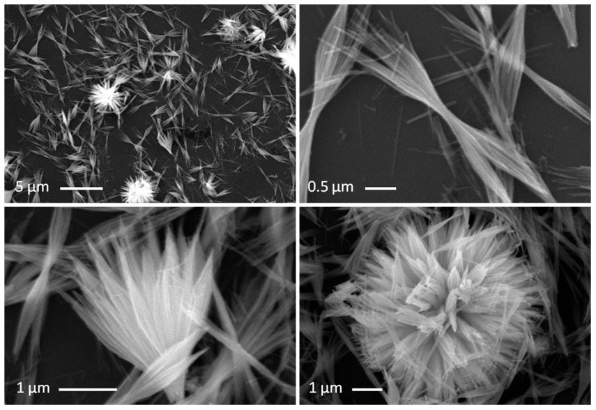
Figure 1: SEM photographs of Sb2S3 nanowires, nanobundles and flower-like structures as-obtained with precursor 1 (top) and 3 (bottom) in DIPB/PVP* solution at 170 °C.

Figure 2: TEM micrographs of Sb2S3 nanobundles and wires formed with precursor 1 in DIPB/PVP* solution at 170 °C.
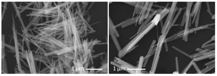
Figure 3: SEM photographs of Sb2Se3 nanowires formed with precursor 4 in OA at 150 °C (left) and 170 °C (right).
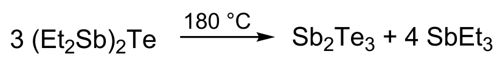
Simultaneous decomposition of two different precursors of the type (Et2Sb)2E (E = S, Se) yielded the ternary material phase Sb2(S,Se)3. The Sb2(S,Se)3 nanowires again grew along the <010> direction (d010 = 0.39 nm) of the Sb2(S,Se)3 stibnite structure (Pnma). Fig. 4 shows a HRTEM image recorded at 250 keV of the Sb2(S,Se)3 nanowire, in which the growth direction is indicated by a double arrow-headed line. The lattice spacings perpendicular to the growth direction, as well as the FFT, that can be indexed as [101], prove the growth direction.
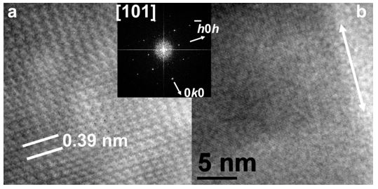
Figure 4: Zoom (a) and amplitude of FFT as inset of the HRTEM image (b) of Sb2(S,Se)3 nanowires formed by simultaneous decomposition of 1 and 2 in DIPB/PVP* at 170 °C in [101] orientation.
Thermal decomposition of the corresponding Te-containing compound [Et2Sb)2Te in non-coordinating solvents gave highly agglomerated particles in a controlled stoichiometric reaction (scheme 1), whereas the presence of capping agents such as PVP yielded isolated Sb2Te3 hexagons.[13]
Scheme 1: Thermally induced decomposition reaction of 1.
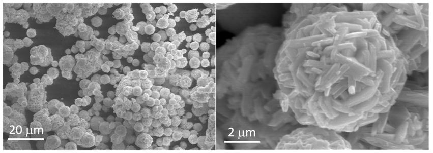
Figure 5: SEM photographs of agglomerated Sb2Te3 nanoplates obtained from thermolysis of 1 in a closed glass ampoule.
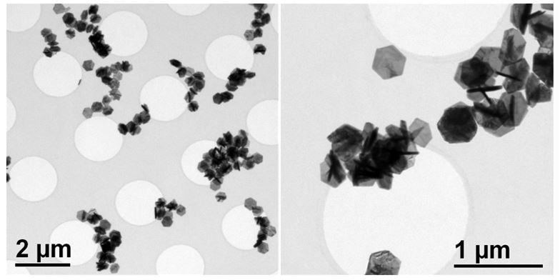
Figure 6: TEM micrographs of Sb2Te3 nanoplates formed in DIPP/PVP* solution at 170 °C.
In order to demonstrate the potential of the as-prepared nanostructures for thermoelectric application, several cold-pressed pellets were characterized with respect to their thermoelectric properties with and without additional temperature anneal. The Seebeck coefficient a showed high values between 145 μV/K and 170 μV/K, which do not have their origin in the size or shape of the nanoplatelets but rather originate from the specific defect chemistry of the material and are a result of a slightly under-stoichiometric tellurium concentration. The under-stoichiometric tellurium concentration results in the formation of Sb-antisite defects, doping the material. Single crystalline Sb2Te3 reference material obtained by travelling heater method has smaller values of the Seebeck coefficient than the ones measured in this study, in the range between around 80 μV/K to 90 μV/K. While the Seebeck coefficients already are in a very favorable range pointing towards ideal composition and defect chemistry of the nanoplates, the relatively low value of the specific electrical conductivity s demonstrates the need for further optimization of the compaction process. For the 'native' sample the electrical conductivity increases from 6 to 9 S/cm, for the annealed powder from 30 to 36 S/cm.
To date the most effective materials for thermoelectric applications near room temperature are bismuth-based materials such as Bi2Te3 and the solid ternary solutions (SbxBi1-x)2Te3 due to their high effective masses, their high electrical conductivities and high Seebeck coefficients combined with glass-like low thermal conductivities. Nanosized Bi2Te3 particles were synthesized in different ways, i.e. by reducing bismuth acetate with oleylamine in dodecanthiole and further treatment with trioctyltellurophosphorane TOPTe, which is a widely used soluble Te-source, at 110 °C. The resulting rhombohedral bismuth-rich Bi2Te3-particles showed reduced thermal conductivity after SPS-treatment and a high power factor (5 µW∙K-2∙cm-1).[14] In addition, hexagonal und rod-shaped Bi2Te3 particles were obtained from the reaction of bismuth nitrate and TOPTe in octadecene and oleic acid and by reaction of BiCl3 and TOPTe in thioglycolic acid in a microwave assisted synthesis.[15]
Even though TOPTe is a suitable Te-precursor for the solution-based synthesis of bismuth tellurides, alternative Te-precursors have been investigated. A general problem in the wet-chemical synthesis of Bi2Te3 nanoparticles is their strong tendency to form so-called antisite defects - the occupation of either Te sites by Bi atoms or Bi sites by Te atoms in the tetradymite lattice, resulting in the formation of either p- or n-doped materials - which strongly influences the carrier concentration and therefore the thermoelectric properties of the resulting material.[16] Moreover, the facile incorporation of excess bismuth into the tetradymite lattice leads to a series of sandwich-like structures of the general form (Bi2)n(Bi2Te3)m, in which the quintuple layers are separated by Bi-bilayers as can be observed in tsumoite BiTe, pilsenite Bi4Te3 and hedleyite Bi7Te3, respectively.
We investigated both single source and dual source approaches for the synthesis of Bi2Te3 nanoparticles. (Et2Bi)2Te, which is readily accessible by insertion reaction of elemental Te into the weak Bi-Bi bond of tetraethyldibismuthine Et4Bi2 in n-pentane at low temperature,[16] was thermolyzed at 80 °C, yielding a black powder which was shown by EDX and XRD to be Bi4Te3.[17] All observed peaks in the PXRD pattern were indexed on the basis of rhombohedral Bi4Te3 (JCPDS 33-216) and the lattice parameters were refined to (a = 4.43(1) Å, c = 41.84(1) Å and V = 415.5(4) Å3). The broad full width half maximum (FWHM) of the peaks indicate a small particle size of roughly 20 nm.
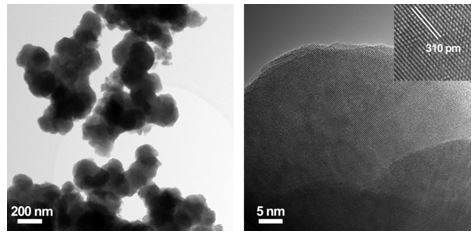
Figure 7: TEM images of Bi4Te3 nanoparticles as obtained by thermal decomposition of 1 at 80 °C in DIPB.
In contrast, thermolysis of in situ generated Et2BiTeEt in DIPB or OA gave pseudo-cubic Bi2Te particles, whose size increase with increasing reaction time. We therefore investigated the reaction of Bi(NMe2)3 with (Et3Si)2Te in different molar ratios.[17] Addition of Bi(NMe2)3 to a solution of Te(SiEt3)2 in DIPB at ambient temperature resulted in an immediate darkening, indicating a fast reaction. Monitoring the reaction in THF-d8 by 1H-NMR spectroscopy proved that the reaction proceeded with elimination of N,N-dimethylaminotriethylsilane Me2NSiEt3 according to the following mechanism:
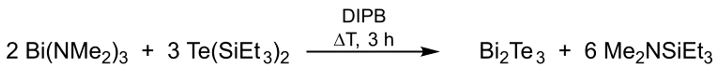
Scheme 2: Reaction of Bi(NMe2)3 and Te(SiEt3)2
The reaction was found to be strongkle dependant on the molar ratio of the starting reagents. As<a consequence, different bismuth telluride phases were obtained simply by changing the molar ratios. The resulting partickles were clearly identified by powder XRD.
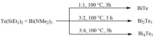
Scheme 3: Summary of the ideal reaction conditions for the formation of phase-pure binary bismuth-tellurium materials.
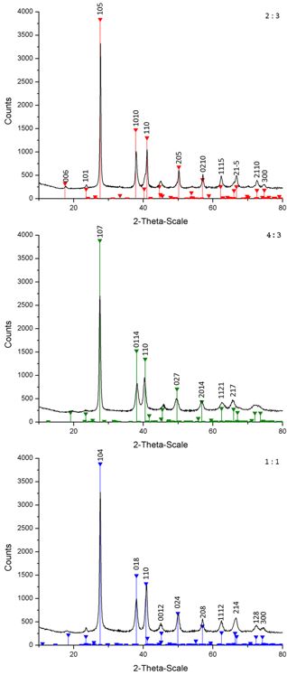
Figure 8: X-ray diffractograms of black powders as obtained by reaction of Bi(NMe2)3 and Te(SiEt3)2 in DIPB in 2:3 (a), 4:3 (b) and 1:1 (c) molar ratios at 100 °C and references (red: Bi2Te3, JCPDS 015-0863; green: Bi4Te3, JCPDS 33-216; blue: BiTe, JCPDS 44-0667).
The Bi2Te3 phase was of particular interest and therefore were further analysed by TEM, showing small pseudo-cubic particles with edge lengths of roughly 40 nm. The SAED pattern was in good agreement with the literature data and clearly shows the formation of phase pure Bi2Te3 as proven by comparison with calculated ED-pattern (ICSD-42546).
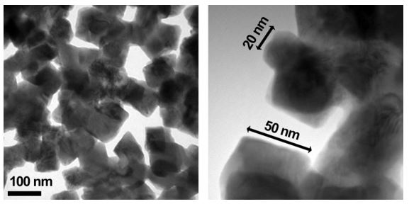
Figure 9: TEM images of Bi2Te3 nanoparticles as obtained by reaction of Bi(NMe2)3 and Te(SiEt3)2 (2:3 molar ratio) in DIPB at 100 °C.
Figure 10 shows the HRTEM image of a Bi2Te3 nanoparticle in [110] zone axis orientation, thus perpendicular to the stacking of the five membered Bi2Te3 building units. Fourier transform of the whole image (Fig. 10b) indicates that the periodicity is perfect and matches perfect with the simulation of the electron diffraction for Bi2Te3 (Fig. 10c). A closer inspection of the thin areas of the sample shows periodic 1 nm stacks perpendicular to the c-axis of Bi2Te3. Each of the stacks has five rows of well resolved contrast maxima, which match the positions of the atoms of Bi2Te3 in this projection. This is illustrated by an overlay of a ball and stick plot of Bi2Te3 in the same orientation and proofs the synthesis of pure Bi2Te3 (Fig. 10a).
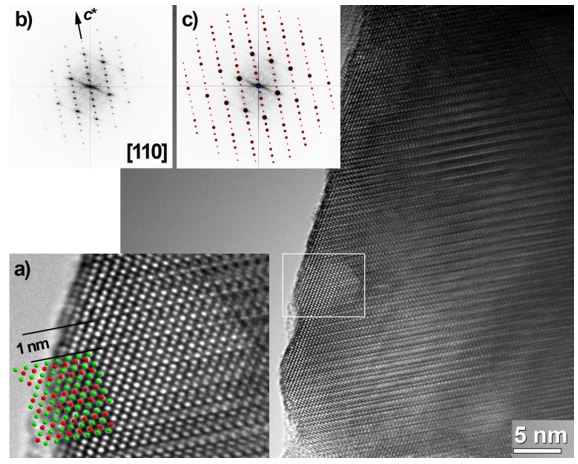
Figure 10: HRTEM image of a Bi2Te3 nanoparticle from Bi(NMe2)3 and Te(SiEt3)2 (2:3 molar ratio) in DIBP at 100 °C. a) Zoom of the boxed area with structure model as overlay; b) Fourier transform of the whole HRTEM image; c) FT with simulation of the diffraction pattern in [110] as overlay.
References
[1] a) J. A. Chang, J. H. Rhee, S. H. Im, Y. H. Lee, H.-J. Kim, S. I. Seok, M. K. Nazeeruddin, M. Grätzel, Nano Lett. 2010, 10, 2609; b) S. H. Im, C.-S. Lim, J. A. Chang, Y. H. Lee, N. Maiti, H.-J. Kim, M. K. Nazeeruddin, M.. Grätzel, S. I. Seok, Nano Lett. 2011, 11, 4789; c) N. Maiti, S. H. Im, C.-S. Lim, S. I. Seok, Dalton Trans. 2012, 41, 11569.
[2] R. Bin Yang, J. Bachmann, E. Pippel, A. Berger, J. Woltersdorf, U. Gösele, K. Nielsch, Adv. Mater. 2009, 21, 3170.
[3] L. G. Gribnyak, T. B. Ivanova, Inorg. Mater. 1987, 23, 478.
[4] N. S. Platakis, H. C. Gatos, Phys. Stat. Sol. 1972, 13, K1.
[5] a) S. Messina, M. T. S. Nair, P. K. Nair, J. Electrochem. Soc. 2009, 156, H327; b) A. M. Fernandez, M. G. Merino, Thin Sol. Films 2000, 366, 202; c) F. T. F. O'Mahony, U. B. Cappel, N. Tokmoldin, T. Lutz, R. Lindblad, H. Rensmo, S. A. Haque, Angew. Chem. Int. Ed. 2013, 52, 12047; d) S. Messina, M. T. S. Nair, P. K. Nair, J. Electrochem. Soc. 2009, 156, H327.
[6] P. Arun, A. G. Vedeshwar, N. C. Mehra, J. Phys. D 1999, 32, 183.
[7] a) A. J. Minnich, M. S. Dresselhaus, Z. F. Ren, G. Chen, Energy Environ. Sci. 2009, 2, 466; b) M. S. Dresselhaus, G. Chen, M. Y. Tang, R. G. Yang, H. Lee, D. Z. Wang, Z. F. Ren, J. P. Fleurial, P. Gogna, Adv. Mater. 2007, 19, 1043.
[8] Harman, T. C.; Taylor, P. J.; Walsh, M. P.; LaForge, B. E. Science 2002, 297, 2229.
[9] Christian, P.; O’Brien, P. J. Mater. Chem. 2005, 15, 4949.
[10] a) F. T. F. O'Mahony, U. B. Cappel, N. Tokmoldin, T. Lutz, R. Lindblad, H. Rensmo, S. A. Haque, Angew. Chem. Int. Ed. 2013, 52, 12047; b) J. R. Castro, K. C. Molloy, Y. Liu, C. S. Lai, Z. Dong, T. J. White, E. R. T. Tiekink, J. Mater. Chem. 2008, 18, 5399; c) W. Lou, M. Chen, X. Wang, W. Liu, Chem. Mater. 2007, 19, 872.
[11] G. Gupta, J. Kim, Dalton Trans. 2013, 42, 8209.
[12] S. Heimann, W. Assenmacher, O. Prymak, S. Schulz, Eur. J. Inorg. Chem. 2015, 14, 2407.
[13] S. Schulz, S. Heimann, J. Friedrich, M. Engenhorst, G. Schierning, W. Assenmacher, Chem. Mater. 2012, 24, 2228.
[14] M. Scheele, N. Oeschler, I. Veremchuk, K.-G. Reinsberg, A.-M. Kreuziger, A. Kornowski, J. Broekaert, C. Klinke, H. Weller, ACS Nano 2010, 4, 4283.
[15] L. Chen, Q. Zhao, X. Ruan, Mater. Lett., 2012, 82, 112; b) R. J. Mehta, Y. Zhang, C. Karthik, B. Singh, R. W. Siegel, T. Borca-Tasciuc, G. Ramanath, Nat. Mater. 2012, 11, 233.
[16] Z. Stary, J. Horak, M. Stordeur, M. Stölzer, J. Phys. Chem. Solids 1988, 49, 29.
[17] S. Heimann, D. Bläser, C. Wölper and S. Schulz, Organometallics 2014, 33, 2295.
[18] G. Bendt, A. Weber, S. Heimann, W. Assenmacher, O. Prymak, S. Schulz, Dalton Trans. 2015, 44, 14272.
For more:4.3.2 Synthesis in ionic liquids
Go Back:4.3.1.2 Group 14 Chalcogenides