Scalable Growth Process
Flexible Light Emitting Elements in 2D
- von Birte Vierjahn
- 14.10.2020
If 80,000 of them were piled on top of each other, the stack would only be as high as a flat sheet of paper. Scientists from the Center for Nanointegration (CENIDE) at the UDE and cooperation partners have developed a layer of tungsten disulfide that is just as thin as three atomic layers – and it is luminous, flexible and also withstands external influences. Several square centimeters of this layer have already been embedded in structural components, but the manufacturing process is scalable beyond that, the trade journal Advanced Optical Materials reports.
The wafer-thin luminescent layer grows on a sapphire base, is then carefully removed with the aid of a lacquer and transferred to the carrier film. The lacquer is then dissolved. In broad terms, this is the manufacturing process the project partners from UDE, RWTH Aachen University and AIXTRON used to develop entire devices from the two-dimensional material. The method can be scaled to much larger areas using the same material and the same device architecture, and this is what makes it interesting from an industrial point of view.
Change the Bending to Change the Light
Led by UDE's Professor Gerd Bacher, lighting elements were created that combine the advantages of different component concepts: The inorganic tungsten disulfide layer is less susceptible to harmful environmental influences such as oxygen or moisture and is also long-term stable. Due to the flexible design, the structure adapts to any shape. But the flexibility has even another advantage: if the film is bent, the crystal lattice of the luminous layer is distorted and the wavelength of the emitted light – and thus the color of the light – changes. Although this difference is not visible to the naked eye, it is easy to detect with measuring instruments.
"This is what makes the elements interesting as sensors, for instance," explains Dr. Tilmar Kümmell from the Bacher working group. "We think they could be used to detect deformation or distortions.” On the other hand, the precise bending of the film would also make it possible to select a specific wavelength for the emitted light.
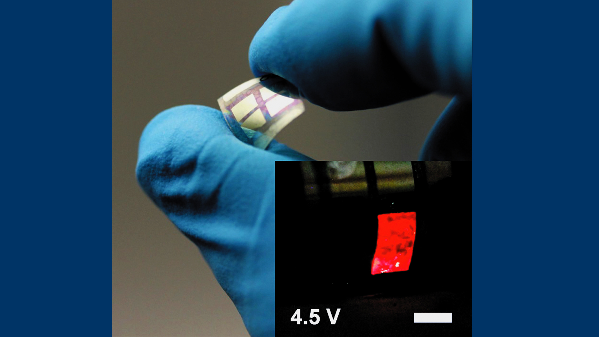
Image: Foil with 1 cm edge length, containing four emitter elements. The insert shows one of them in operation. The scalebar is 2 mm.
Original Publication:
D. Andrzejewski, R. Oliver, Y. Beckmann, A. Grundmann, M. Heuken, H. Kalisch, A. Vescan, T. Kümmell, G. Bacher
„Flexible large-area light-emitting devices based on WS2 monolayers“
Advanced Optical Materials 2020, 2000694
https://doi.org/10.1002/adom.202000694
Further Information:
Dr. Tilmar Kümmell, Electronic Materials and Nanostructures, +49 203/37 9-3403, tilmar.kuemmell@uni-due.de
Editor: Birte Vierjahn, +49 203/37 9-8176, birte.vierjahn@uni-due.de